CM1233 查看數據表(PDF) - California Micro Devices Corp
零件编号
产品描述 (功能)
生产厂家
CM1233
California Micro Devices Corp

CM1233 Datasheet PDF : 10 Pages
| |||
CM1233
Application Information
CM1233 Application and Guidelines
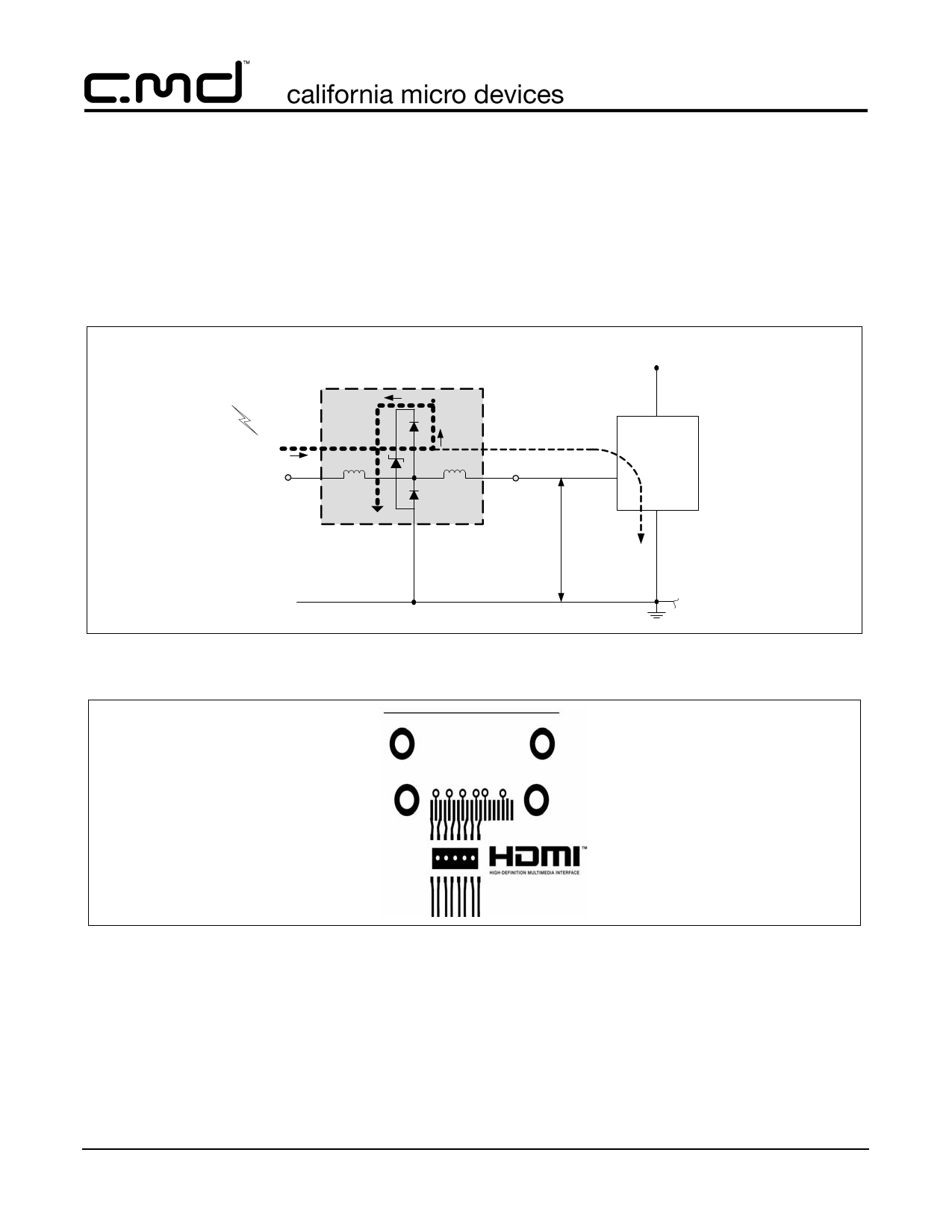
As a general rule, the CM1233 ESD protection array should be located as close as possible to the point of entry of
expected electrostatic discharges with minimum PCB trace lengths to the ground planes and between the signal
input and the ESD device to minimize stray series inductance.
Path of ESD
current pulse
(IESD)
Channel
Output
CM1233
Line Being
Protected
Channel
Input
VCL
VCC
Circuitry Under
Protection
VN
Ground Rail
Figure 8. Application of Positive ESD Pulse Between Input Channel and Ground
Figure 9. Typical PCB Layout
Additional Information
See also California Micro Devices Application Note AP209, “Design Considerations for ESD Protection,” in the
Applications section at www.calmicro.com.
© 2008 California Micro Devices Corp. All rights reserved.
8
490 N. McCarthy Blvd., Milpitas, CA 95035-5112 ● Tel: 408.263.3214 ● Fax: 408.263.7846 ● www.cmd.com
Issue A – 03/18/08
Share Link: