CM3106-12SH 查看數據表(PDF) - California Micro Devices Corp
零件编号
产品描述 (功能)
生产厂家
CM3106-12SH Datasheet PDF : 11 Pages
| |||
Application Information
VDDQ
AVIN
PVIN
CAVIN
47µF
CM3106
VDDQ
AVIN
VREF
VSENSE
CREF
0.1µF
VREF
PVIN
CPVIN
47µF
GND
VTT
VTT
CTT
220µF
CM3106
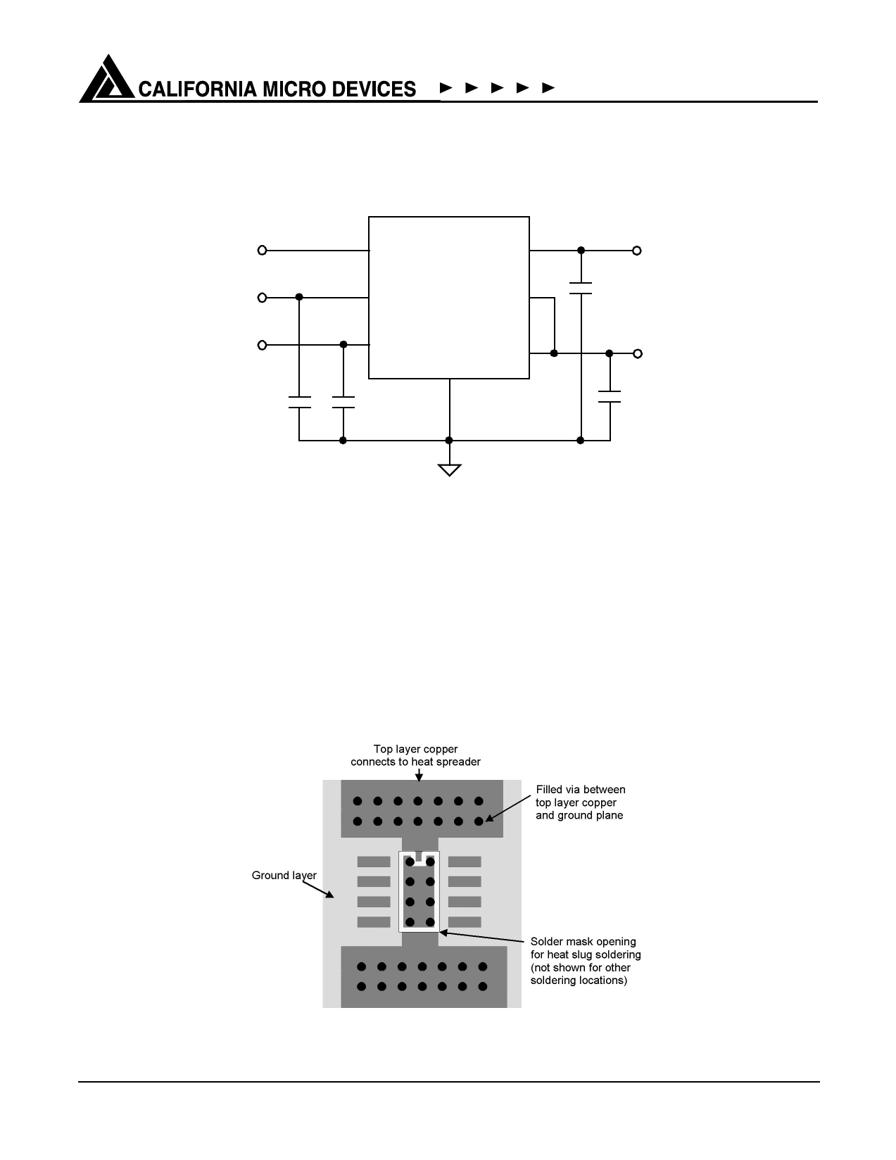
Figure 15. Typical Application Circuit
PCB Layout Considerations
The CM3106-12SB has a heat spreader attached to
the underneath of the PSOP-8 package in order for
heat to be transferred much easier from the package to
the PCB. The heat spreader is a copper pad of dimen-
sions just smaller than the package itself. By position-
ing the matching pad on the PCB top layer to connect
to the spreader during manufacturing, the heat will be
transferred between the two pads. The drawing below
shows the recommended PCB layout. Note that there
are six vias on either side to allow the heat to dissipate
into the ground and power planes on the inner layers of
the PCB. Vias can be placed underneath the chip, but
this can cause blockage of the solder. The ground and
power planes should be at least 2 sq in. of copper by
the vias. It also helps dissipation to spread if the chip is
positioned away from the edge of the PCB, and not
near other heat dissipating devices. A good thermal
link from the PCB pad to the rest of the PCB will ensure
a thermal link from the CM3106 package to ambient,
θJA, of around 40°C/W.
Figure 16. Recommended Heat Sink PCB Layout
© 2004 California Micro Devices Corp. All rights reserved.
02/02/04 430 N. McCarthy Blvd., Milpitas, CA 95035-5112
L Tel: 408.263.3214 L Fax: 408.263.7846 L www.calmicro.com
9
Share Link: 