CM3205 查看數據表(PDF) - California Micro Devices Corp
零件编号
产品描述 (功能)
生产厂家
CM3205 Datasheet PDF : 10 Pages
| |||
PRELIMINARY
CM3205
Application Information (cont’d)
where VADJ = 1.215V (±-1%). For best regulator stabil-
ity, we recommend that R1 and R2 not exceed 10-kΩ
each.
Shutdown
Pin 1 (ADJSD) also serves as a shutdown pin. When
pin 1 is pulled high, > (VIN - 1.2V), the VDDQ output is
turned off and both source and sink MOSFET’s of the
VTT regulator are set to a high impedance state. During
shutdown, the quiescent current is reduced to less than
3mA, independent of output load.
It is recommended that a 1N914 or equivalent low leak-
age diode be placed between Pin 1 and an external
shutdown signal to prevent interference with the ADJ
pin’s normal operation. When the diode anode is pulled
low, or left open, the CM3205 is again enabled.
Current Limit, Foldback and Over-temperature Pro-
tection
The CM3205 features internal current limiting with ther-
mal protection. During normal operation, VDDQ limits
the output current to approximately 8A and VTT limits
the output current to approximately ±2A. When VTT is
current limiting into a hard short circuit, the output cur-
rent folds back to a lower level, about 1.5A, until the
over-current condition ends. While current limiting is
designed to prevent gross device failure, care should
be taken not to exceed the power dissipation ratings of
the package. If the junction temperature of the device
exceeds 170-°C (typical), the thermal protection cir-
cuitry triggers and shuts down both outputs. Once the
junction temperature has cooled to below about
120-°C, the CM3205 returns to normal operation.
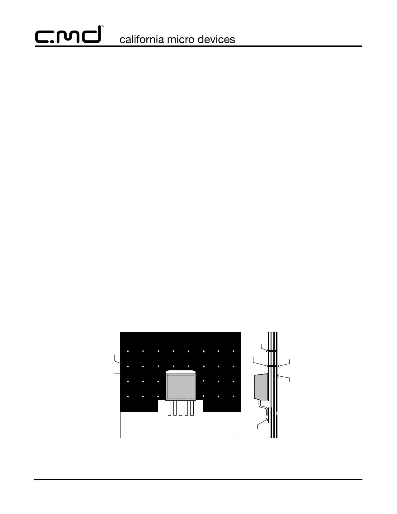
Thermal Considerations
Both the TO-252 and the TO-263 packages provide a
very effective thermal conduction path from the silicon
junction into the PC board to which it is mounted. See
Figure 2 below. These surface mount packages have a
large metal tab that solders to the PC board, where the
ground plane can serve as heatsink. This metal tab
connects internally to GND (pin 3). A top-layer ground
plane is the best in terms of convection air-cooling, a
bottom-layer ground plane is less effective, and a mid-
dle layer ground plane of a multiple-layer PC board is
the least effective.
We recommend the metal tab of CM3205 be soldered
to a minimum of 3 square inches of ground plane on
the top side of the PC board. Use 20 or more plate-
through vias to connect the top layer ground plane to
ground planes on other layers.
When measured in accordance to JEDEC JESD51-3,
under natural convection without forced airflow, the
Theta junction-to-air (θja) resistance is approximately
48-°C/watt for the CM3205-00TN (TO-263-5), and
55-°C/watt for the CM3205-00TP (TO-252-5).
Vias (0.3mm
Diameter)
Ground
Plane
(TOP VIEW)
(SIDE VIEW)
Via
Top
Ground
Plane
Via (0.3mm
Diameter)
Bottom
Ground
Plane
Power Trace
Figure 2. Thermal Layout
© 2006 California Micro Devices Corp. All rights reserved.
8 490 N. McCarthy Blvd., Milpitas, CA 95035-5112 l Tel: 408.263.3214 l Fax: 408.263.7846 l www.cmd.com
05/08/06
Share Link: 