GS8170DW18C-250 查看數據表(PDF) - Giga Semiconductor
零件编号
产品描述 (功能)
生产厂家
GS8170DW18C-250 Datasheet PDF : 36 Pages
| |||
Preliminary
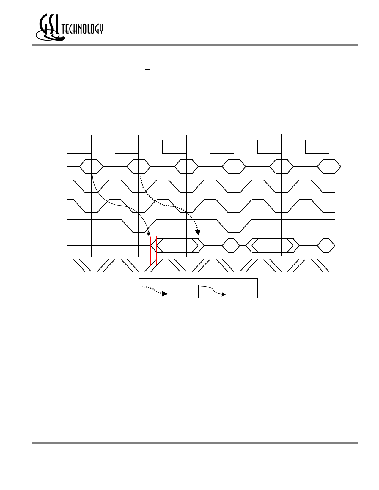
GS8170DW18/36/72C-333/300/250
Write Operations
Write operation occurs when the following conditions are satisfied at the rising edge of clock: All three chip enables (E1, E2, and
E3) are active, the write enable input signal (W) is asserted low, and ADV is asserted low.
Double Late Write
Double Late Write means that Data In is required on the third rising edge of clock. Double Late Write is used to implement Pipeline
mode NBT SRAMs.
SigmaRAM Double Late Write with Pipelined Read
Read
W rite
Read
W rite
Read
CK
Address
A
B
C
D
E
F
ADV
/E1
/W
DQ
QA
DB
QC
DD
CQ
Key
Hi-Z
Access
Rev: 1.00d 6/2002
11/36
© 2002, Giga Semiconductor, Inc.
Specifications cited are design targets and are subject to change without notice. For latest documentation contact your GSI representative.
Share Link: 