GS8170DW18C-300I 查看數據表(PDF) - Giga Semiconductor
零件编号
产品描述 (功能)
生产厂家
GS8170DW18C-300I Datasheet PDF : 36 Pages
| |||
Preliminary
GS8170DW18/36/72C-333/300/250
The character of the applications for fast synchronous SRAMs in networking systems are extremely diverse. ΣRAMs have been
developed to address the broad variety of applications in the networking market in a manner that can be supported with a unified
development and manufacturing infrastructure. ΣRAMs address each of the bus protocol options commonly found in networking
systems. This allows the ΣRAM to find application in radical shrinks and speed-ups of existing networking chip sets that were
designed for use with older SRAMs, like the NBT, Late Write, or Double Data Rate SRAMs, as well as with new chip sets and
ASICs that employ the Echo Clocks and realize the full potential of the ΣRAMs.
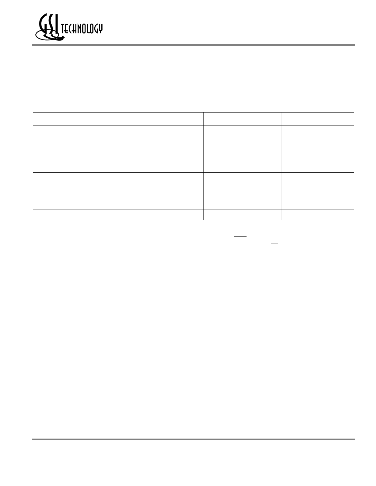
Mode Selection Truth Table Standard
L6 M6 J6 Name
0 0 0 Σ1x1Ef
0 0 1 Σ1x1Lf
010
0 1 1 Σ1x2Lp
1 0 0 Σ1x1Ep
1 0 1 Σ1x1Dp
1 1 0 Σ1x1Lp
111
Function
Early Write, Flow through Read
Late Write, Flow through Read
RFU
DDR
Early Write, Pipeline Read
Double Late Write, Pipeline Read
Late Write, Pipeline Read
RFU
Analogous to...
Flow through Burst RAM
Flow through NBT SRAM
Double Data Rate SRAM
Pipelined Burst RAM
Pipelined NBT SRAM
Pipelined Late Write SRAM
—
In This Data Sheet?
No
No
n/a
No
No
Yes
No
n/a
All address, data and control inputs (with the exception of PE2, PE3, ZQ, and the mode pins, L6, M6, J6) are synchronized to
rising clock edges. Read and write operations must be initiated with the Advance/Load pin (ADV) held low, in order to load the
new address. Device activation is accomplished by asserting all three of the Chip Enable inputs (E1, E2, and E3). Deassertion of
any one of the Enable inputs will deactivate the device. It should be noted that ONLY deactivation of the RAM via E2 and/or
E3 deactivates the Echo Clocks, CQ1–CQ2.
Rev: 1.00d 6/2002
9/36
© 2002, Giga Semiconductor, Inc.
Specifications cited are design targets and are subject to change without notice. For latest documentation contact your GSI representative.
Share Link: 