GS8180D18D-333 查看數據表(PDF) - Giga Semiconductor
零件编号
产品描述 (功能)
生产厂家
GS8180D18D-333 Datasheet PDF : 27 Pages
| |||
Preliminary
GS8180D18D-333/300/250/200
Σ2x2B4 SigmaQuad SRAM DDR Read
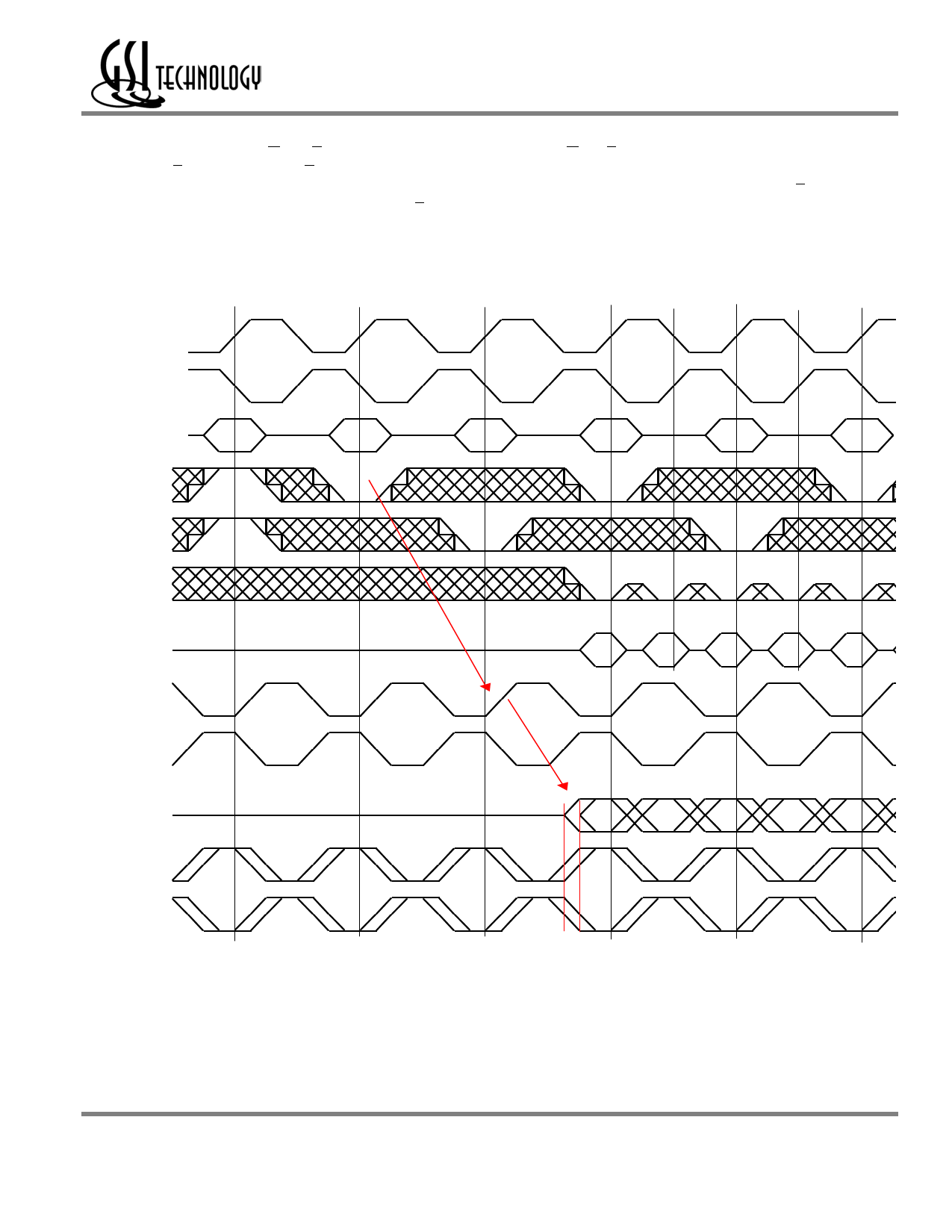
The status of the Address Input, W, and R pins are sampled at each rising edge of K. W and R high causes chip disable. A low on the Read
Enable-bar pin, R, begins a read cycle. R is always ignored if the previous command loaded was a read command. The four resulting data output
transfers begin after the next rising edge of the K clock. Data is clocked out by the next rising edge of the C, the rising edge of C after that, the
next rising edge of C, and finally by the next rising edge of C.
Σ2x2B4 Double Data Rate SigmaQuad SRAM Read First
Dwg Rev. G
No Op
Read
Write
Read
Write
Read
K
/K
Address
XX
B
C
D
E
F
/R
/W
/BWx
D
DC0
DC1
DC2
DC3
DE0
C
/C
QB0
QB1
QB2
QB3
QD0
Q
CQ
/CQ
Rev: 2.00f 6/2002
5/27
© 2002, Giga Semiconductor, Inc.
Specifications cited are design targets and are subject to change without notice. For latest documentation contact your GSI representative.
Share Link: 