CS5205-2GDP3 查看數據表(PDF) - ON Semiconductor
零件编号
产品描述 (功能)
生产厂家
CS5205-2GDP3 Datasheet PDF : 8 Pages
| |||
CS5205−2
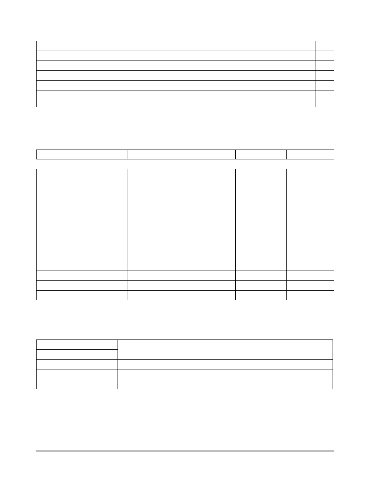
MAXIMUM RATINGS*
Parameter
Value
Unit
Supply Voltage, VCC
Operating Temperature Range
17
V
−40 to +70
°C
Junction Temperature
150
°C
Storage Temperature Range
−60 to +150 °C
Lead Temperature Soldering:
Wave Solder (through hole styles only) Note 1 260 Peak
°C
Reflow (SMD styles only) Note 2 230 Peak
°C
1. 10 second maximum.
2. 60 second maximum above 183°C
*The maximum package power dissipation must be observed.
ELECTRICAL CHARACTERISTICS (CIN = 10 mF, COUT = 22 mF Tantalum, VIN − VOUT = 3.0 V, VIN ≤ 10 V, 0°C ≤ TA ≤ 70°C,
TJ ≤ +150°C, unless otherwise specified, Ifull load = 5.0 A)
Characteristic
Test Conditions
Min
Typ
Max
Unit
Fixed Output Voltage
Output Voltage (Notes 3 and 4)
Line Regulation
Load Regulation (Notes 3 and 4)
Dropout Voltage (Note 5)
Current Limit
Quiescent Current
Thermal Regulation
Ripple Rejection
Temperature Stability
VIN − VOUT = 1.5 V;
0 ≤ IOUT ≤ 5.0 A
1.5 V ≤ VIN − VOUT ≤ 6.0 V; IOUT = 10 mA
VIN − VOUT = 1.5 V; 10 mA ≤ IOUT ≤ 5.0 A
IOUT = 5.0 A
VIN − VOUT = 3.0 V; TJ ≥ 25°C
VIN − VOUT = 9.0 V
VIN ≤ 9.0 V; IOUT = 10 mA
30 ms Pulse, TA = 25°C
f = 120 Hz; IOUT = 5.0 A
−
1.47
(−2.0%)
−
−
−
5.5
−
−
−
−
−
1.50
0.04
0.08
1.2
8.5
1.0
5.0
0.003
75
0.5
1.53
(+2.0%)
0.20
0.40
1.3
−
−
10
−
−
−
V
%
%
V
A
A
mA
%/W
dB
%
RMS Output Noise (%VOUT)
Thermal Shutdown
10 Hz ≤ f ≤ 10 kHz
−
−
0.003
150
180
−
%/VOUT
−
°C
Thermal Shutdown Hysteresis
−
−
25
−
°C
3. Load regulation and output voltage are measured at a constant junction temperature by low duty cycle pulse testing. Changes in output
voltage due to thermal gradients or temperature changes must be taken into account separately.
4. Specifications apply for an external Kelvin sense connection at a point on the output pin 1/4” from the bottom of the package.
5. Dropout voltage is a measurement of the minimum input/output differential at full load.
PACKAGE PIN DESCRIPTION
Package Pin Number
TO−220−3
D2PAK−3
1
1
2
2
3
3
Pin Symbol
GND
VOUT
VIN
Ground connection.
Function
Regulated output voltage (case).
Input voltage.
http://onsemi.com
2
Share Link: 