CS8147 查看數據表(PDF) - ON Semiconductor
零件编号
产品描述 (功能)
生产厂家
CS8147 Datasheet PDF : 12 Pages
| |||
CS8147
DEFINITION OF TERMS
Dropout Voltage – The input–output voltage differential
at which the circuit ceases to regulate against further
reduction in input voltage. Measured when the output
voltage has dropped 100 mV from the nominal value
obtained at 14 V input, dropout voltage is dependent upon
load current and junction temperature.
Current Limit – Peak current that can be delivered to the
output.
Input Voltage – The DC voltage applied to the input
terminals with respect to ground.
Input Output Differential – The voltage difference
between the unregulated input voltage and the regulated
output voltage for which the regulator will operate.
Line Regulation – The change in output voltage for a
change in the input voltage. The measurement is made under
conditions of low dissipation or by using pulse techniques
such that the average chip temperature is not significantly
affected.
Load Regulation – The change in output voltage for a
change in load current at constant chip temperature.
Long Term Stability – Output voltage stability under
accelerated life–test conditions after 1000 hours with
maximum rated voltage and junction temperature.
Output Noise Voltage – The rms AC voltage at the
output, with constant load and no input ripple, measured
over a specified frequency range.
Quiescent Current – The part of the positive input
current that does not contribute to the positive load current.
The regulator ground lead current.
Ripple Rejection – The ratio of the peak–to–peak input
ripple voltage to the peak–to–peak output ripple voltage.
Temperature Stability of VOUT – The percentage
change in output voltage for a thermal variation from room
temperature to either temperature extreme.
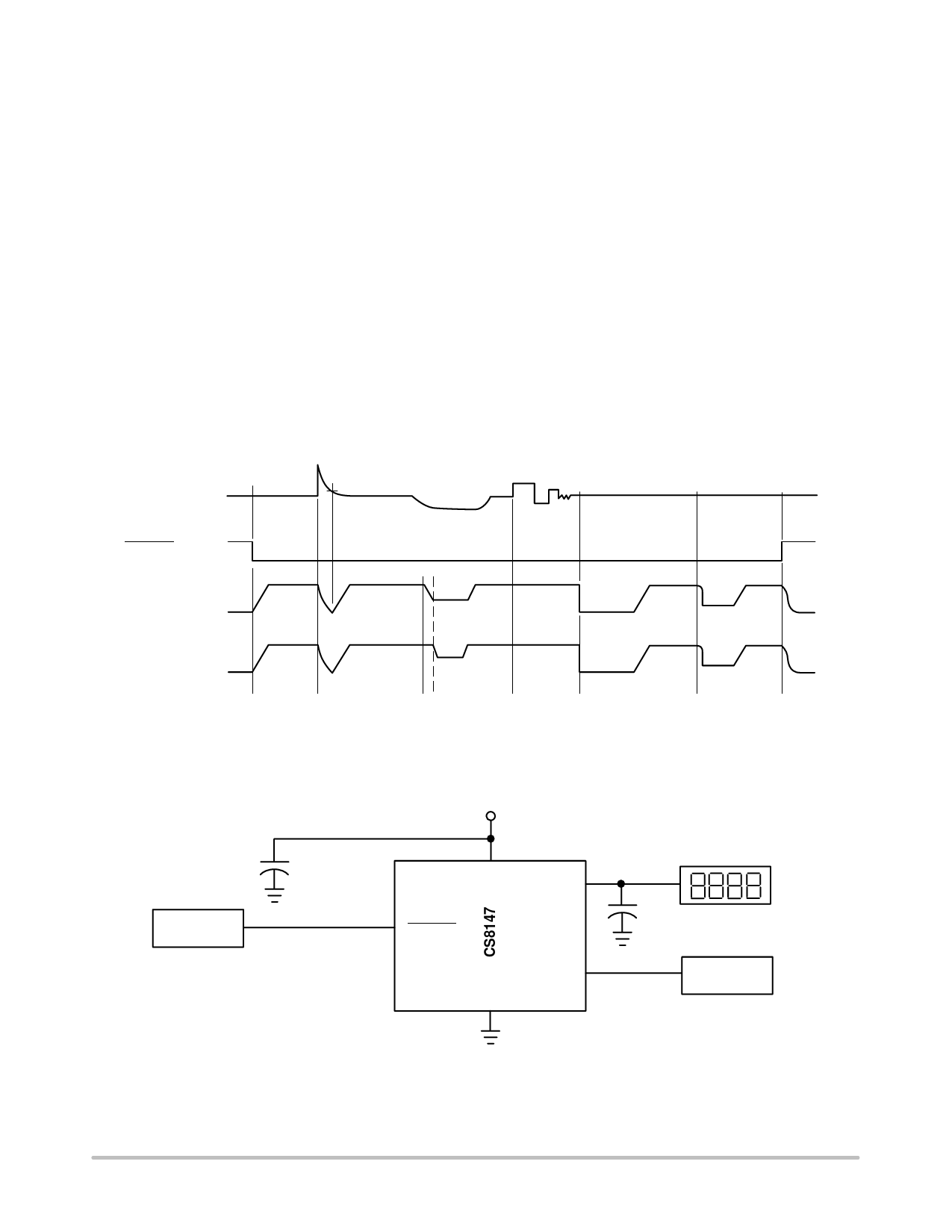
60 V
31 V
26 V
14V
VIN 14 V
5.0 V
ENABLE 2.0 V
0.8 V
VOUT1 0 V
VOUT2
0V
10 V
5.0 V
10 V
5.0 V
5.0 V 3.0 V
10 V
0V
5.0 V
0V
Turn
On
Load
Dump
Low VIN
Line
Noise, Etc.
VOUT
Short
Circuit
Figure 14. Typical Circuit Waveform
10 V
10 V
0V
0V
5.0 V
5.0 V
0V
0V
Thermal
Shutdown
Turn
Off
Control
C1*
0.1 µF
VIN
ENABLE
VOUT1
GND
VOUT2
10V
C2**
10 µF
5.0V
Tuner IC
* C1 is required if the regulator is located away from the power source filter.
** C2 is required for stability.
Figure 15. Test & Applications Circuit
http://onsemi.com
6
Share Link: 