CS8156 查看數據表(PDF) - ON Semiconductor
零件编号
产品描述 (功能)
生产厂家
CS8156 Datasheet PDF : 11 Pages
| |||
CS8156
appear. Record the values of load current and ESR that cause
the greatest oscillation. This represents the worst case load
conditions for the regulator at low temperature.
Step 4: Maintain the worst case load conditions set in step
3 and vary the input voltage until the oscillations increase.
This point represents the worst case input voltage
conditions.
Step 5: If the capacitor is adequate, repeat steps 3 and 4 with
the next smaller valued capacitor. A smaller capacitor will
usually cost less and occupy less board space. If the output
oscillates within the range of expected operating conditions,
repeat steps 3 and 4 with the next larger standard capacitor
value.
Step 6: Test the load transient response by switching in
various loads at several frequencies to simulate its real
working environment. Vary the ESR to reduce ringing.
Step 7: Raise the temperature to the highest specified
operating temperature. Vary the load current as instructed in
step 5 to test for any oscillations.
Once the minimum capacitor value with the maximum
ESR is found for each output, a safety factor should be added
to allow for the tolerance of the capacitor and any variations
in regulator performance. Most good quality aluminum
electrolytic capacitors have a tolerance of ±20% so the
minimum value found should be increased by at least 50%
to allow for this tolerance plus the variation which will occur
at low temperatures. The ESR of the capacitors should be
less than 50% of the maximum allowable ESR found in step
3 above.
Repeat steps 1 through 7 with C3, the capacitor on the
other output.
Calculating Power Dissipation in a
Dual Output Linear Regulator
The maximum power dissipation for a dual output
regulator (Figure 20) is
PD(max) + NJVIN(max) * VOUT1(min)NjIOUT1(max) )
NJVIN(max) * VOUT2(min)NjIOUT2(max) ) VIN(max)IQ (1)
where:
VIN(max) is the maximum input voltage,
VOUT1(min) is the minimum output voltage from VOUT1,
VOUT2(min) is the minimum output voltage from VOUT2,
IOUT1(max) is the maximum output current, for the
application,
IOUT2(max) is the maximum output current, for the
application, and
IQ is the quiescent current the regulator consumes at
IOUT(max).
Once the value of PD(max) is known, the maximum
permissible value of RΘJA can be calculated:
RQJA
+
150°C *
PD
TA
(2)
The value of RΘJA can be compared with those in the
package section of the data sheet. Those packages with
RΘJA’s less than the calculated value in equation 2 will keep
the die temperature below 150°C.
In some cases, none of the packages will be sufficient to
dissipate the heat generated by the IC, and an external
heatsink will be required.
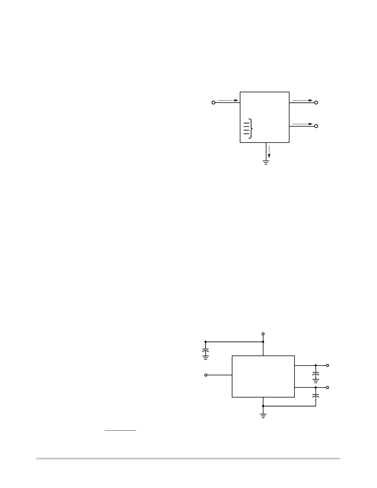
IIN
VIN
Smart
Regulator
Control
Features
IOUT1
IOUT2
VOUT1
VOUT2
IQ
Figure 20. Dual Output Regulator With Key
Performance Parameters Labeled.
Heat Sinks
A heat sink effectively increases the surface area of the
package to improve the flow of heat away from the IC and
into the surrounding air.
Each material in the heat flow path between the IC and the
outside environment will have a thermal resistance. Like
series electrical resistances, these resistances are summed to
determine the value of RΘJA:
RQJA + RQJC ) RQCS ) RQSA
(3)
where:
RΘJC = the junction−to−case thermal resistance,
RΘCS = the case−to−heatsink thermal resistance, and
RΘSA = the heatsink−to−ambient thermal resistance.
RΘJC appears in the package section of the data sheet. Like
RΘJA, it too is a function of package type. RΘCS and RΘSA
are functions of the package type, heatsink and the interface
between them. These values appear in heat sink data sheets
of heat sink manufacturers.
C1*
0.1 μF
VIN
CS8156
ENABLE
VOUT1
GND
VOUT2
+ C2**
22 μF
+ C3**
22 μF
* C1 is required if the regulator is far from power supply filter.
** C2, C3 required for stability.
Figure 21. Test & Application Circuit
http://onsemi.com
8
Share Link: 