CXA1851 查看數據表(PDF) - Sony Semiconductor
零件编号
产品描述 (功能)
生产厂家
CXA1851 Datasheet PDF : 12 Pages
| |||
CXA1851N
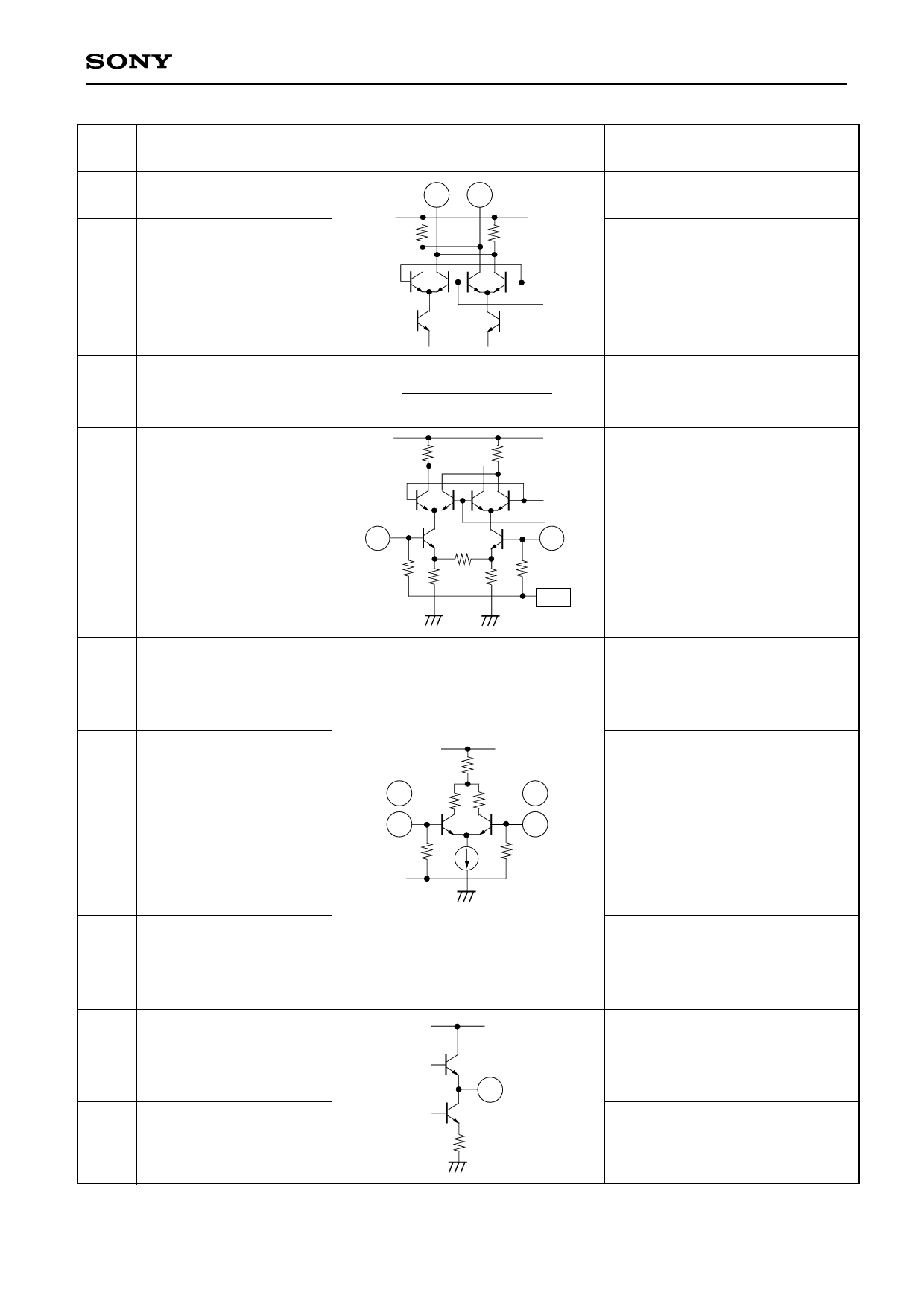
Pin No. Symbol
10 MIX OUT1
Typical pin
voltage (V)
2.3
11 MIX OUT2
2.3
12 GND
0.0
13 IF BYPASS
1.03
14 IF INPUT
1.03
15 OSC INPUT
1.8
(for UP
CONV.)
16 OSC
1.8
BYPASS
(for UP
CONV.)
17 OSC
1.85
BYPASS
(for DOWN
CONV.)
18 OSC
1.85
BYPASS
(for DOWN
CONV.)
19 Vcc
2.7 to 4.5
(for DOWN
CONV.)
20 IF OUTPUT 1.45
Equivalent circuit
10 11
14
13
REG
15
16
18
17
Description
MIX output pin for the up
converter.
MIX output pin for the up
converter. Connect an approxi-
mately 4.7 nH chip inductor and
an approximately 3.5 pF chip
capacitor between this pin and
Pin 10 to form a tank circuit.
GND pin for the oscillator buffer
amplifier and mixer blocks of the
up converter.
IF input by-pass pin for the up
converter.
IF input pin for the up converter.
Because of high impedance, an
external matching circuit is
necessary which consists of a 220
nH chip inductor and an
approximately 1.5 pF chip
capacitor.
Oscillator input pin for the up
converter. A matching circuit
consisting of a 51Ω resistor is
necessary.
Oscillator input by-pass pin for the
up converter.
Oscillator input by-pass pin for the
down converter.
Oscillator input pin for the down
converter. A matching circuit
consisting of a 51Ω resistor is
necessary.
Power supply for the down
converter.
20
IF output pin for the down
converter.
—3—
Share Link: 