CXA2108 查看數據表(PDF) - Sony Semiconductor
零件编号
产品描述 (功能)
生产厂家
CXA2108 Datasheet PDF : 28 Pages
| |||
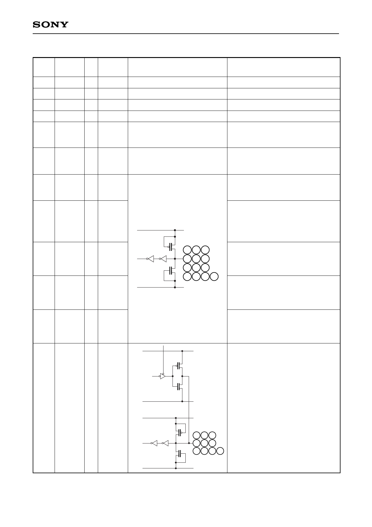
Pin Description
Pin
No.
9, 56
Symbol
AGND
Reference
I/O voltage
level
— GND
8, 57 AVCC — 5V (Typ.)
12, 22, 42 DGND — GND
23, 43 DVCC — 5V (Typ.)
5, 60,
66, 70, IGND
75, 79
— GND
10,
53, 54
NC
—
21 CLK
I CMOS
51 XRST I CMOS
11 MODE I CMOS
34 to 41,
44
A0 to 8
I CMOS
45 A9
I CMOS
24 to 33 D0 to 9 I/O CMOS
CXA2108Q
Equivalent circuit
Description
Analog GND.
Analog power supply.
Digital GND.
Digital power supply.
GND for driver output.
DVCC
21 51 11
34 35 36
37 38 39
40 41 44 45
DGND
DVCC
Open.
This pin is not connected with the
internal circuits.
Clock input.
Driver operation is synchronized with
this clock.
Reset input.
The IC is initialized by inputting low
level. However, the memory is not
initialized. Input high level during
normal operation.
Output mode switching.
Upper/Lower mode for low level input.
Upper/Lower/RGB mode for high level
input. (See the Description of Operation.)
Address input.
These pins are used to input the internal
RAM (luminance data, brightness data
and drive current data RAM) address.
RAM selection.
The luminance data RAM is selected
when this pin is low, and the drive
current data RAM when high.
DGND
DVCC
24 25 26
27 28 29
30 31 32 33
Data I/O.
These pins are used to input and
output data to and from the internal
RAM (luminance data, brightness data
and drive current data RAM). See
Table 1. Read/Write Switching
Condition Correspondence Table for
the data I/O switching conditions.
DGND
–4–
Share Link: 