CY62256LL-55SNE 查看數據表(PDF) - Cypress Semiconductor
零件编号
产品描述 (功能)
生产厂家
CY62256LL-55SNE Datasheet PDF : 12 Pages
| |||
CY62256
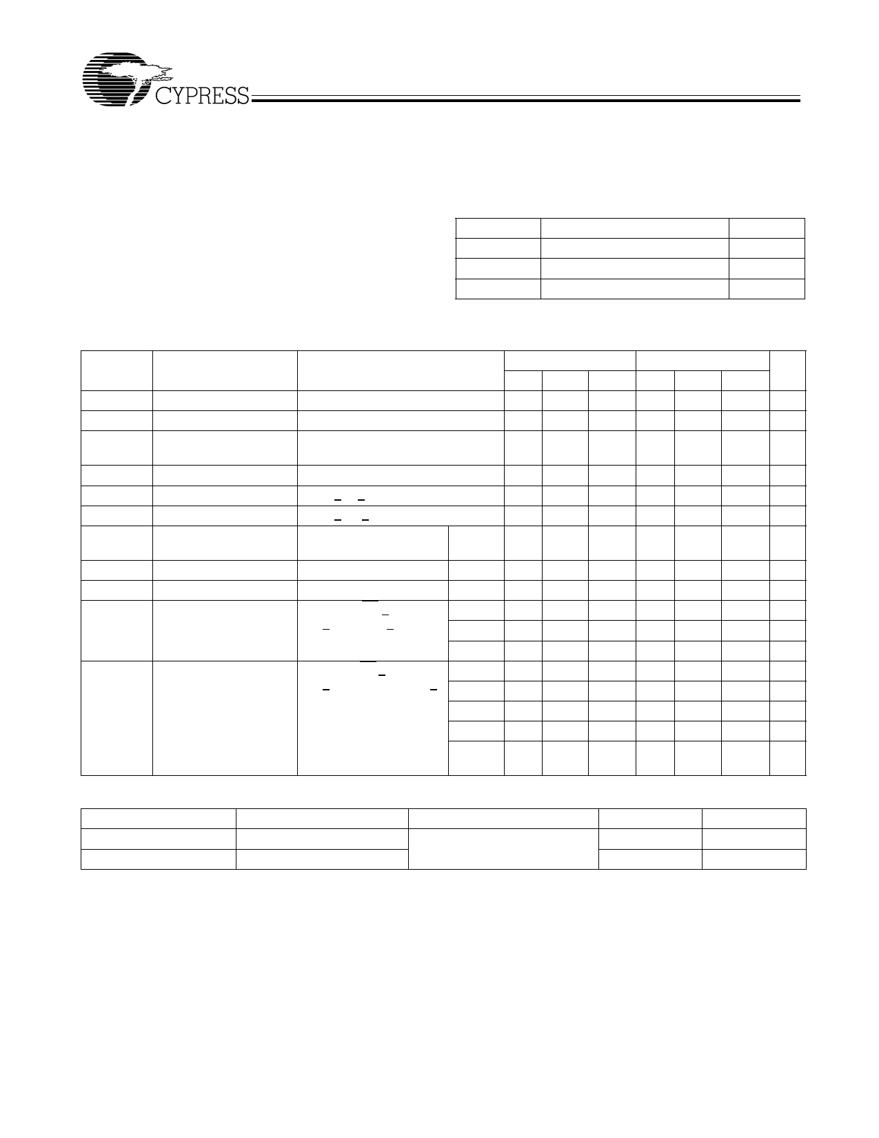
Maximum Ratings
(Above which the useful life may be impaired. For user guide-
lines, not tested.)
Storage Temperature ................................. –65°C to +150°C
Ambient Temperature with
Power Applied..............................................-55°C to +125°C
Supply Voltage to Ground Potential
(Pin 28 to Pin 14) ........................................... –0.5V to +7.0V
DC Voltage Applied to Outputs
in High-Z State[3] ....................................–0.5V to VCC + 0.5V
DC Input Voltage[3].................................–0.5V to VCC + 0.5V
Electrical Characteristics Over the Operating Range
Output Current into Outputs (LOW)............................. 20 mA
Static Discharge Voltage.......................................... > 2001V
(per MIL-STD-883, Method 3015)
Latch-up Current.................................................... > 200 mA
Operating Range
Range
Ambient Temperature (TA)[4]
Commercial
0°C to +70°C
Industrial
–40°C to +85°C
Automotive
–40°C to +125°C
VCC
5V ± 10%
5V ± 10%
5V ± 10%
Parameter
Description
Test Conditions
CY62256−55
Min. Typ.[2] Max.
VOH
Output HIGH Voltage VCC = Min., IOH = −1.0 mA
2.4
VOL
Output LOW Voltage VCC = Min., IOL = 2.1 mA
VIH
Input HIGH Voltage
2.2
0.4
VCC
+0.5V
VIL
Input LOW Voltage
–0.5
0.8
IIX
Input Leakage Current GND < VI < VCC
–0.5
+0.5
IOZ
Output Leakage Current GND < VO < VCC, Output Disabled –0.5
+0.5
ICC
VCC Operating Supply VCC = Max., IOUT = 0 mA,
Current
f = fMAX = 1/tRC
28 55
L
25 50
LL
25 50
ISB1
Automatic CE
Max. VCC, CE > VIH,
Power-down Current— VIN > VIH or VIN < VIL, f = L
TTL Inputs
fMAX
LL
0.5
2
0.4 0.6
0.3 0.5
ISB2
Automatic CE
Max. VCC, CE > VCC − 0.3V
Power-down Current— VIN > VCC − 0.3V, or VIN < L
CMOS Inputs
0.3V, f = 0
LL
1
5
2
50
0.1
5
LL - Ind’l
0.1 10
LL -
Auto
0.1 15
CY62256−70
Min. Typ.[2] Max.
2.4
0.4
2.2
VCC
+0.5V
–0.5
0.8
–0.5
+0.5
–0.5
+0.5
28
55
25
50
25
50
0.5
2
0.4 0.6
0.3 0.5
1
5
2
50
0.1
5
0.1 10
Unit
V
V
V
V
µA
µA
mA
mA
mA
mA
mA
mA
mA
µA
µA
µA
µA
Capacitance[5]
Parameter
Description
Test Conditions
CIN
COUT
Input Capacitance
Output Capacitance
TA = 25°C, f = 1 MHz,
VCC = 5.0V
Notes:
3. VIL (min.) = −2.0V for pulse durations of less than 20 ns.
4. TA is the “Instant-On” case temperature.
5. Tested initially and after any design or process changes that may affect these parameters.
Max.
Unit
6
pF
8
pF
Document #: 38-05248 Rev. *C
Page 3 of 12
Share Link: 