7C1325B-100 查看數據表(PDF) - Cypress Semiconductor
零件编号
产品描述 (功能)
生产厂家
7C1325B-100 Datasheet PDF : 17 Pages
| |||
CY7C1325B
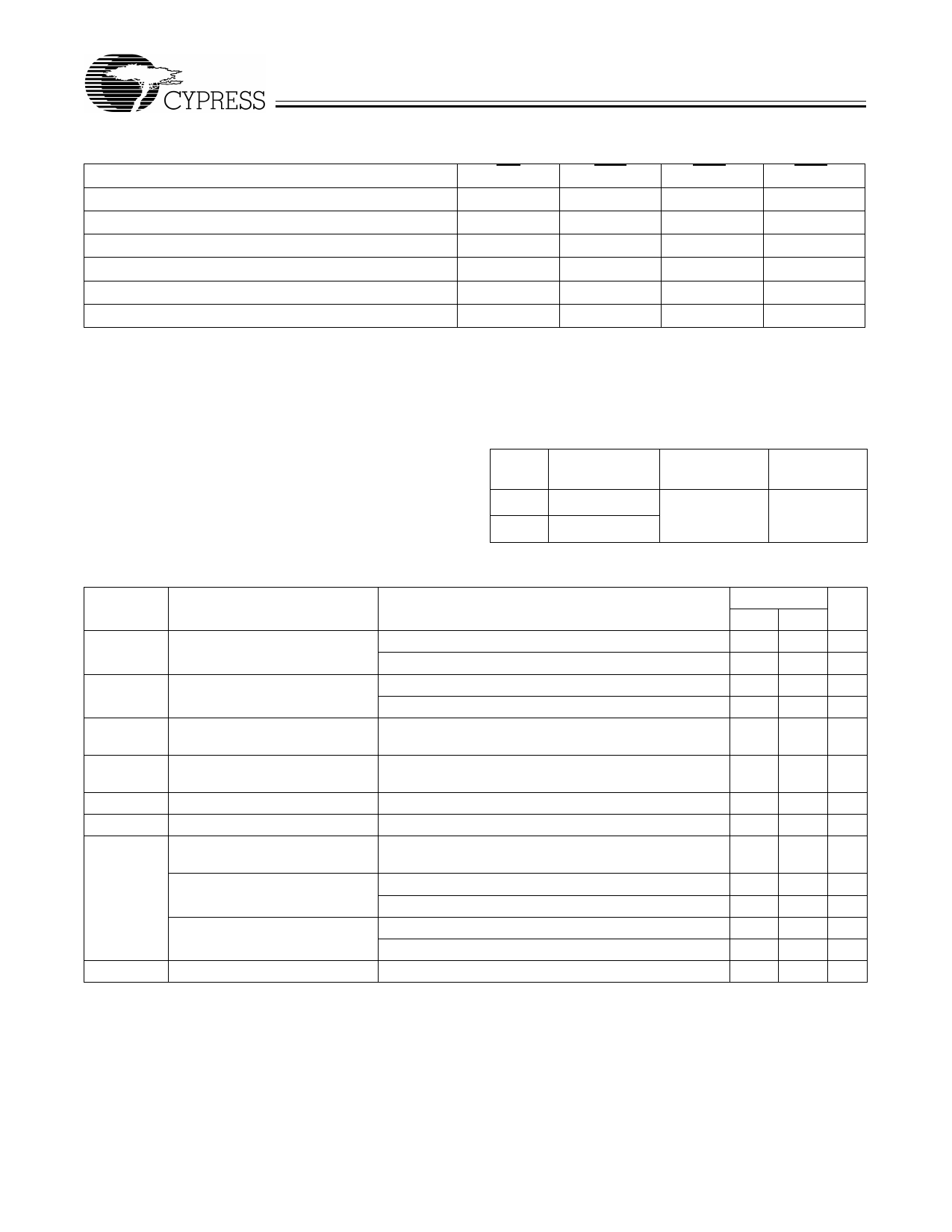
Write Cycle Descriptions[1, 2, 3, 4]
Function
Read
Read
Write Byte 0 - DQ[7:0] and DP0
Write Byte 1 - DQ[15:8] and DP1
Write All Bytes
Write All Bytes
GW
BWE
BWS1
BWS0
1
1
X
X
1
0
1
1
1
0
1
0
1
0
0
1
1
0
0
0
0
X
X
X
Maximum Ratings
(Above which the useful life may be impaired. For user guide-
lines, not tested.)
Storage Temperature ...................................–65°C to +150°C
Ambient Temperature with
Power Applied ...............................................–55°C to +125°C
Supply Voltage on VDD Relative to GND................ –0.5V to +4.6V
DC Voltage Applied to Outputs
in High Z State[5]...............................................–0.5V to VDD + 0.5V
DC Input Voltage[5]...........................................–0.5V to VDD + 0.5V
Current into Outputs (LOW)......................................... 20 mA
Static Discharge Voltage .......................................... >2001V
(per MIL-STD-883, Method 3015)
Latch-Up Current .................................................... >200 mA
Operating Range
Ambient
Range Temperature[6]
VDD
VDDQ
Com’l 0°C to +70°C 3.135V to 3.6V 2.375V to VDD
Ind’l
–40°C +70°C
Electrical Characteristics Over the Operating Range
Parameter
Description
VOH
Output HIGH Voltage
VOL
Output LOW Voltage
VIH
Input HIGH Voltage
Test Conditions
VDDQ = 3.3V, VDD = Min., IOH = –4.0 mA
VDDQ = 2.5V, VDD = Min., IOH = –2.0 mA
VDDQ = 3.3V, VDD = Min., IOL = 8.0 mA
VDDQ = 2.5V, VDD = Min., IOL = 2.0 mA
VDDQ = 3.3V
VIH
Input HIGH Voltage
VDDQ = 2.5V
VIL
Input LOW Voltage[5]
VIL
Input LOW Voltage[5]
VDDQ = 3.3V
VDDQ = 2.5V
IX
Input Load Current
GND ≤ VI ≤ VDDQ
(except ZZ and MODE)
Input Current of MODE
Input = VSS
Input = VDDQ
Input Current of ZZ
Input = VSS
Input = VDDQ
IOZ
Output Leakage Current
GND ≤ VI ≤ VDD, Output Disabled
Notes:
4. When a write cycle is detected, all I/Os are three-stated, even during byte writes.
5. Minimum voltage equals –2.0V for pulse durations of less than 20 ns.
6. TA is the case temperature.
7C1325B
Min. Max. Unit
2.4
V
2.0
V
0.4 V
0.7 V
2.0 VDD + V
0.3V
1.7 VDD + V
0.3V
–0.3 0.8 V
–0.3 0.7 V
−1
1 µA
–30
µA
5 µA
–5
µA
30 µA
–5
5 µA
7
Share Link: 