7C1325B-100 查看數據表(PDF) - Cypress Semiconductor
零件编号
产品描述 (功能)
生产厂家
7C1325B-100 Datasheet PDF : 17 Pages
| |||
CY7C1325B
Electrical Characteristics Over the Operating Range (continued)
7C1325B
Parameter
IOS
IDD
Description
Output Short Circuit Current[7]
VDD Operating Supply Current
Test Conditions
VDD = Max., VOUT = GND
VDD = Max., IOUT = 0 mA,
f = fMAX= 1/tCYC
8.5-ns cycle, 117 MHz
10-ns cycle, 100 MHz
Min.
Max. Unit
–300 mA
350 mA
325 mA
ISB1
Automatic CE Power-Down
Max. VDD, Device Deselected, 8.5-ns cycle, 117 MHz
Current—TTL Inputs
VIN ≥ VIH or VIN ≤ VIL, f = fMAX,
10-ns cycle, 100 MHz
inputs switching
125 mA
110 mA
ISB2
Automatic CE Power-Down
Max. VDD, Device Deselected, All speeds
Current—CMOS Inputs
VIN ≥ VDD – 0.3V or VIN ≤ 0.3V,
f = 0, inputs static
10 mA
ISB3
Automatic CE Power-Down
Max. VDD, Device Deselected, 8.5-ns cycle, 117 MHz
Current—CMOS Inputs
VIN ≥ VDDQ – 0.3V or VIN ≤ 0.3V, 10-ns cycle, 100 MHz
f = fMAX, inputs switching
ISB4
Automatic CE Power-Down
Max. VDD, Device Deselected, All speeds
Current—TTL Inputs
VIN ≥ VDD – 0.3V or VIN ≤ 0.3V,
f = 0, inputs static
95 mA
85 mA
30 mA
Capacitance[8]
Parameter
CIN
CI/O
Description
Input Capacitance
I/O Capacitance
Test Conditions
TA = 25°C, f = 1 MHz,
VDD = 5.0V
Max.
Unit
4
pF
4
pF
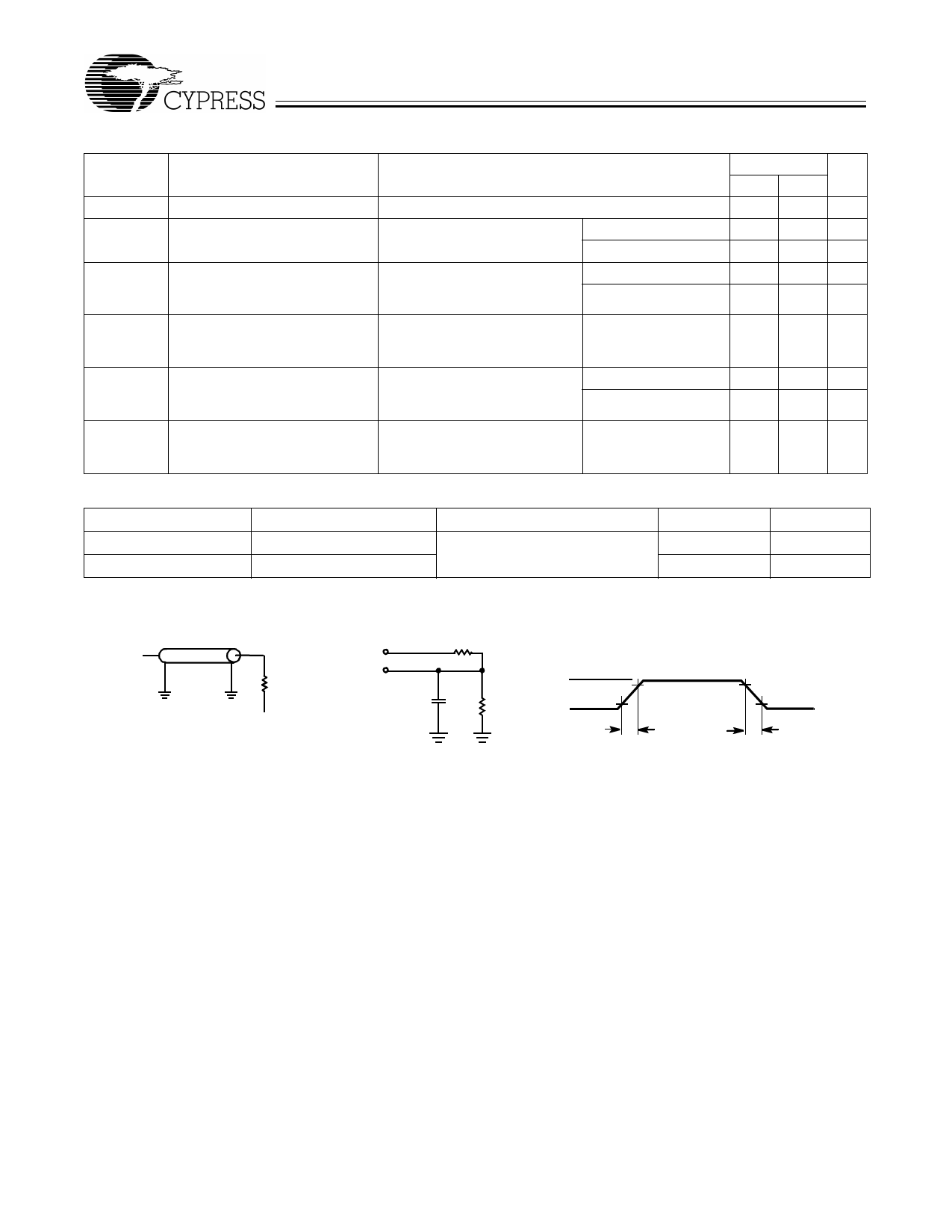
AC Test Loads and Waveforms
OUTPUT
Z0 =50Ω
RL =50Ω
VL =1.5V
(a)
2.5V
OUTPUT
5 pF
INCLUDING
JIGAND
SCOPE
R1
R2
2.5V
GND
10%
ALL INPUT PULSES
90%
90%
10%
(b)[9]
Rise Time: 1 V/ns
Fall Time: 1 V/ns
Notes:
7. Not more than one output should be shorted at one time. Duration of the short circuit should not exceed 30 seconds.
8. Tested initially and after any design or process changes that may affect these parameters.
9. R1=1667Ω and R2=1538Ω for IOH/IOL=–4/8 mA, R1=521Ω and R2=481Ω for IOH/IOL=–2/2 mA.
8
Share Link: 