CY7C401 查看數據表(PDF) - Cypress Semiconductor
零件编号
产品描述 (功能)
生产厂家
CY7C401 Datasheet PDF : 13 Pages
| |||
1CY 7C40 2
CY7C401/CY7C403
CY7C402/CY7C404
Features
• 64 x 4 (CY7C401 and CY7C403)
64 x 5 (CY7C402 and CY7C404)
High-speed first-in first-out memory (FIFO)
• Processed with high-speed CMOS for optimum
speed/power
• 25-MHz data rates
• 50-ns bubble-through time—25 MHz
• Expandable in word width and/or length
• 5-volt power supply ± 10% tolerance, both commercial
and military
• Independent asynchronous inputs and outputs
• TTL-compatible interface
• Output enable function available on CY7C403 and
CY7C404
• Capable of withstanding greater than 2001V electro-
static discharge
• Pin compatible with MMI 67401A/67402A
Functional Description
The CY7C401 and CY7C403 are asynchronous first-in
first-out (FIFOs) organized as 64 four-bit words. The CY7C402
and CY7C404 are similar FIFOs organized as 64 five-bit
64 x 4 Cascadable FIFO
64 x 5 Cascadable FIFO
words. Both the CY7C403 and CY7C404 have an output en-
able (OE) function.
The devices accept 4- or 5-bit words at the data input (DI0 –
DIn) under the control of the shift in (SI) input. The stored
words stack up at the output (DO0 – DOn) in the order they
were entered. A read command on the shift out (SO) input
causes the next to last word to move to the output and all data
shifts down once in the stack. The input ready (IR) signal acts
as a flag to indicate when the input is ready to accept new data
(HIGH), to indicate when the FIFO is full (LOW), and to provide
a signal for a cascading. The output ready (OR) signal is a flag
to indicate the output contains valid data (HIGH), to indicate
the FIFO is empty (LOW), and to provide a signal for cascad-
ing.
Parallel expansion for wider words is accomplished by logical-
ly ANDing the IR and OR signals to form composite signals.
Serial expansion is accomplished by tying the data inputs of
one device to the data outputs of the previous device. The IR
pin of the receiving device is connected to the SO pin of the
sending device, and the OR pin of the sending device is con-
nected to the SI pin of the receiving device.
Reading and writing operations are completely asynchronous,
allowing the FIFO to be used as a buffer between two digital
machines of widely differing operating frequencies. The
25-MHz operation makes these FIFOs ideal for high-speed
communication and controller applications.
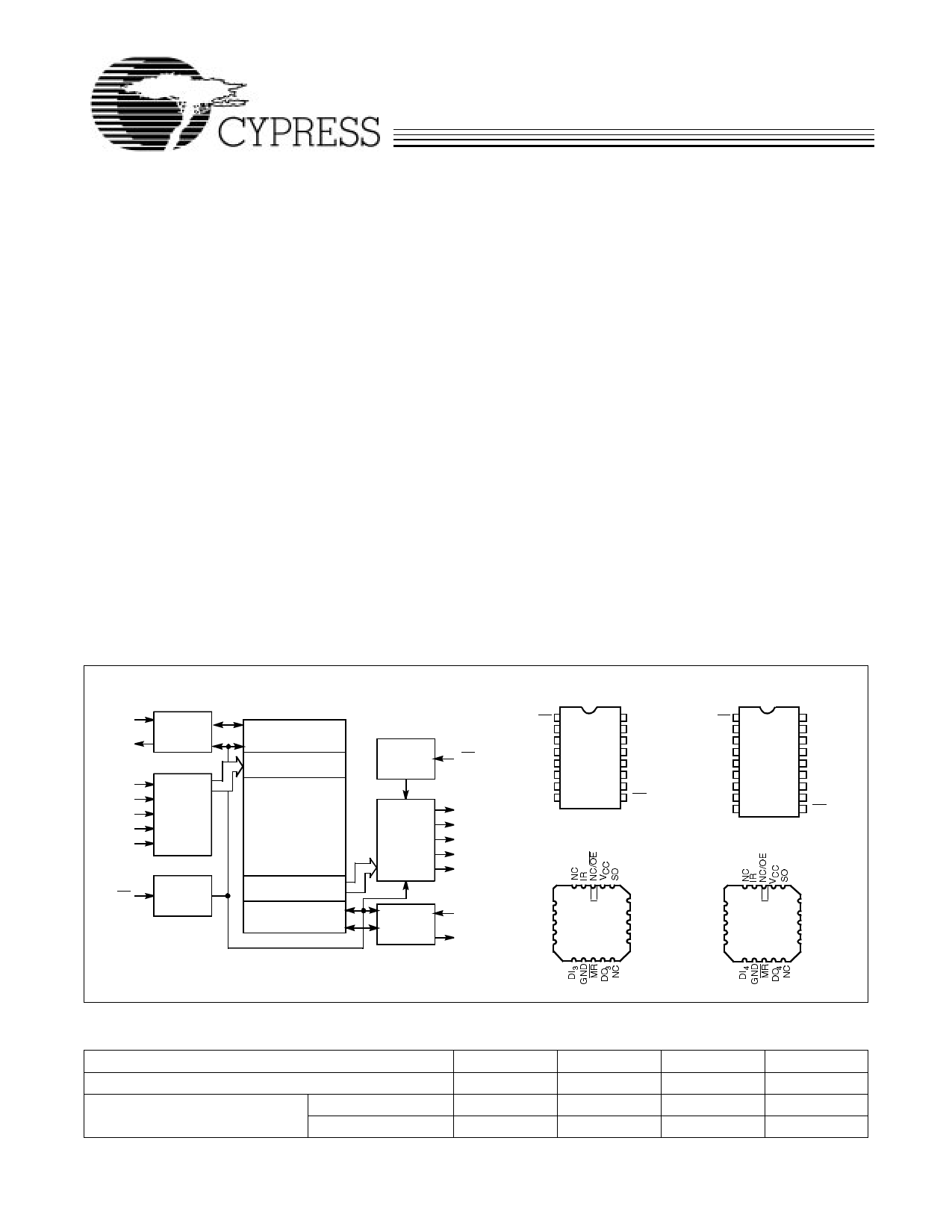
Logic Block Diagram
SI
INPUT
CONTROL
IR
LOGIC
DI 0
DI 1
DI 2
DI 3
(DI 4)
DATAIN
WRITE POINTER
WRITE MULTIPLEXER
MEMORY
ARRAY
MR
MASTER
RESET
READ MULTIPLEXER
READ POINTER
OUTPUT
ENABLE
DATAIN
Pin Configurations
(CY7C401) NC
(CY7C403) OE
IR
OE
DO0
SI
DI 0
DI 1
DI 2
DI 3
GND
DO1
DIP
1
16
2
15
3
14
4
5
CCYY77CC4400131123
6
11
7
10
8
9
VCC
SO
OR
DO 0
DO 1
DO 2
DO 3
MR
C401–2
(CY7C402) NC
(CY7C404) OE
IR
SI
DI 0
DI 1
DI 2
DI 3
DI 4
GND
DO2
LCC
DO3
(DO 4)
DIP
1
18
2
17
3
4
CCYY77CC4400241156
5
14
6
13
7
12
8
11
9
10
VCC
SO
OR
DO 0
DO 1
DO 2
DO 3
DO 4
MR
C401–4
LCC
OUTPUT
SO
CONTROL
LOGIC
OR
C401–1
SI
DI 0
DI 1
DI 2
NC
3 2 1 2019
4
18
5
6
7
CY7C401
CY7C403
17
16
15
8
14
910111213
NC
OR
DO 0
DO 1
DO 2
3 2 1 2019
SI 4
18 OR
DI 0
DI 1
DI 2
5
17
6 CY7C402 16
7 CY7C404 15
DO 0
DO 1
DO 2
DI 3 8
14 DO 3
910111213
C401–3
C401–5
Selection Guide
Operating Frequency (MHz)
Maximum Operating
Current (mA)
Commercial
Military
7C401/2–5
5
75
7C40X–10
10
75
90
7C40X–15
15
75
90
7C40X–25
25
75
90
Cypress Semiconductor Corporation • 3901 North First Street • San Jose • CA 95134 • 408-943-2600
March 1986 – Revised April 1995
Share Link: 