CY7C401 查看數據表(PDF) - Cypress Semiconductor
零件编号
产品描述 (功能)
生产厂家
CY7C401 Datasheet PDF : 13 Pages
| |||
CY7C401/CY7C403
CY7C402/CY7C404
Maximum Ratings
(Above which the useful life may be impaired. For user guide-
lines, not tested.)
Storage Temperature ................................. –65°C to +150°C
Ambient Temperature with
Power Applied............................................. –55°C to +125°C
Supply Voltage to Ground Potential ............... –0.5V to +7.0V
DC Voltage Applied to Outputs
in High Z State ............................................... –0.5V to +7.0V
DC Input Voltage............................................ –3.0V to +7.0V
Power Dissipation ..........................................................1.0W
Output Current, into Outputs (LOW)............................ 20 mA
Static Discharge Voltage ........................................... >2001V
(per MIL-STD-883, Method 3015)
Latch-Up Current ..................................................... >200 mA
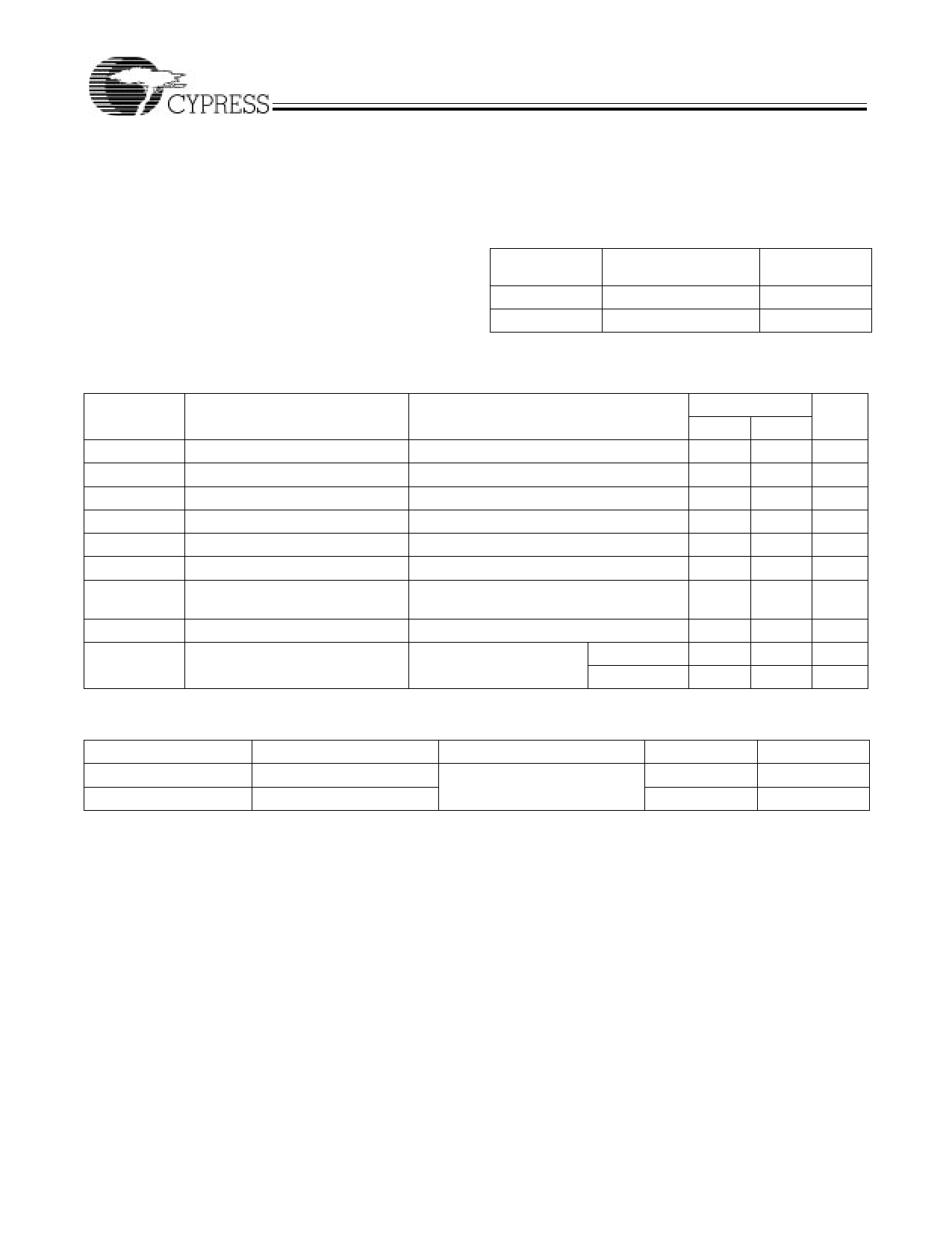
Operating Range
Range
Commercial
Military[1]
Ambient
Temperature
0°C to +70°C
–55°C to +125°C
VCC
5V ±10%
5V ±10%
Electrical Characteristics Over the Operating Range (Unless Otherwise Noted)[2]
Parameter
VOH
VOL
VIH
VIL
IIX
VCD[3]
IOZ
Description
Output HIGH Voltage
Output LOW Voltage
Input HIGH Voltage
Input LOW Voltage
Input Leakage Current
Input Diode Clamp Voltage[3]
Output Leakage Current
IOS
Output Short Circuit Current[4]
ICC
Power Supply Current
Test Conditions
VCC = Min., IOH = –4.0 mA
VCC = Min., IOL = 8.0 mA
GND ≤ VI ≤ VCC
7C40X–10, 15, 25
Min. Max. Unit
2.4
V
0.4
V
2.0
6.0
V
– 3.0
0.8
V
– 10
+10
µA
GND ≤ VOUT ≤ VCC, VCC = 5.5V
– 50
+50
µA
Output Disabled (CY7C403 and CY7C404)
VCC = Max., VOUT = GND
VCC = Max., IOUT = 0 mA
Commercial
Military
– 90
mA
75
mA
90
mA
Capacitance[5]
Parameter
Description
Test Conditions
Max.
Unit
CIN
COUT
Input Capacitance
Output Capacitance
TA = 25°C, f = 1 MHz,
VCC = 4.5V
5
pF
7
pF
Notes:
1. TA is the “instant on” case temperature.
2. See the last page of this specification for Group A subgroup testing information.
3. The CMOS process does not provide a clamp diode. However, the FIFO is insensitive to –3V dc input levels and –5V undershoot pulses of less than 10 ns
(measured at 50% output).
4. For test purposes, not more than one output at a time should be shorted. Short circuit test duration should not exceed 30 seconds.
5. Tested initially and after any design or process changes that may affect these parameters.
2
Share Link: 