CY8C52(2011_03) ТЪЦуюІТЋИТЊџУАе№╝ѕPDF№╝Ѕ - Cypress Semiconductor
жЏХС╗Ху╝ќтЈи
С║ДтЊЂТЈЈУ┐░ (тіЪУЃй)
ућЪС║Дтјѓт«Х
CY8C52 Datasheet PDF : 94 Pages
| |||
PRELIMINARY
PSoC® 5: CY8C52 Family Datasheet
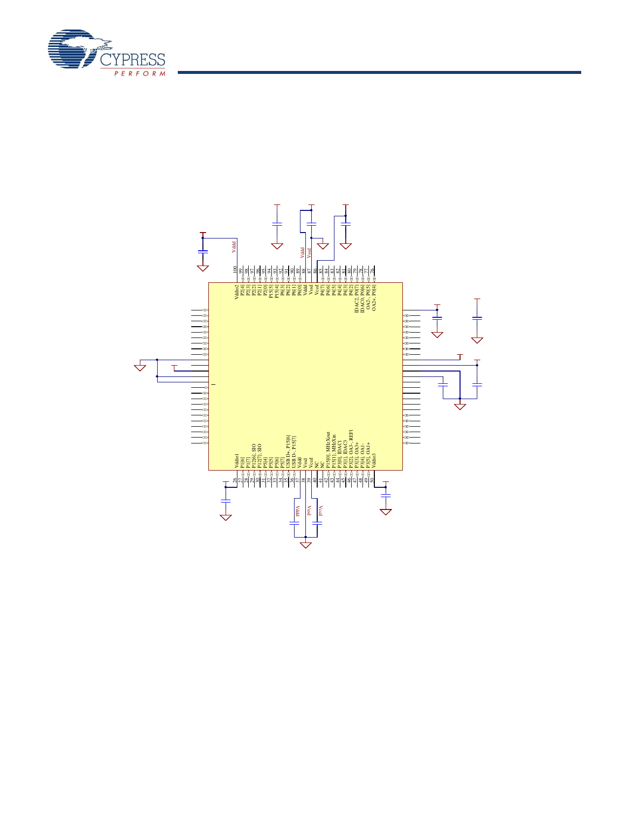
Figure 2-4. Example PCB Layout for 100-pin TQFP Part for Optimal Analog Performance
Vssa
Vddd
Vssd
Vdda
Vssd
Plane
Vssa
Plane
3. Pin Descriptions
IDAC0. Low resistance output pin for high IDAC.
Extref0, Extref1. External reference input to the analog system.
GPIO. General purpose I/O pin provides interfaces to the CPU,
digital peripherals, analog peripherals, interrupts, LCD segment
drive, and CapSense[6].
Ind. Inductor connection to boost pump.
kHz XTAL: Xo, kHz XTAL: Xi. 32.768 kHz crystal oscillator pin.
MHz XTAL: Xo, MHz XTAL: Xi. 4 to 25 MHz crystal oscillator
pin. If a crystal is not used, then Xi must be shorted to ground
and Xo must be left floating.
nTRST. Optional JTAG Test Reset programming and debug port
connection to reset the JTAG connection.
SIO. Special I/O provides interfaces to the CPU, digital
peripherals and interrupts with a programmable high threshold
voltage, analog comparator, high sink current, and high
impedance state when the device is unpowered.
SWDCK. Serial wire debug clock programming and debug port
connection.
SWDIO. Serial wire debug Input and output programming and
debug port connection.
TCK. JTAG Test Clock programming and debug port connection.
TDI. JTAG Test Data In programming and debug port
connection.
TDO. JTAG Test Data Out programming and debug port
connection.
TMS. JTAG Test Mode Select programming and debug port
connection.
TRACECLK. Cortex-M3 TRACEPORT connection, clocks
TRACEDATA pins.
TRACEDATA[3:0]. Cortex-M3 TRACEPORT connections,
output data.
SWV. Single wire viewer output.
USBIO, D+. Provides D+ connection directly to a USB 2.0 bus.
May be used as a digital I/O pin; it is powered from VDDD instead
of from a VDDIO. Pins are Do Not Use (DNU) on devices without
USB.
USBIO, D-. Provides D- connection directly to a USB 2.0 bus.
May be used as a digital I/O pin; it is powered from VDDD instead
of from a VDDIO. Pins are Do Not Use (DNU) on devices without
USB.
VBOOST. Power sense connection to boost pump.
VBAT. Battery supply to boost pump.
VCCA. Output of analog core regulator and input to analog core.
Requires a 1 ┬хF capacitor to VSSA. Regulator output not for
external use.
VCCD. Output of digital core regulator and input to digital core.
The two VCCD pins must be shorted together, with the trace
between them as short as possible, and a 1-┬хF capacitor to
VSSD; see Power System on page 21. Regulator output not for
external use.
VDDA. Supply for all analog peripherals and analog core
regulator. VDDA must be the highest voltage present on the
device. All other supply pins must be less than or equal to VDDA.
Notes
6. GPIOs with opamp outputs are not recommended for use with CapSense.
Document Number: 001-66236 Rev. **
Page 8 of 94
[+] Feedback
Share Link: 