J112 查看數據表(PDF) - Calogic, LLC
零件编号
产品描述 (功能)
生产厂家
J112 Datasheet PDF : 1 Pages
| |||
CORPORATION
N-Channel JFET Switch
J111 - J113 / SST111 – SST113
FEATURES
Low Cost
• Automated Insertion Package
• Low Insertion Loss
• No Offset or Error Voltage Generated By Closed Switch
• - Purely Resistive
- High Isolation Resistance From Driver
Fast Switching
•• Short Sample and Hold Aperture Time
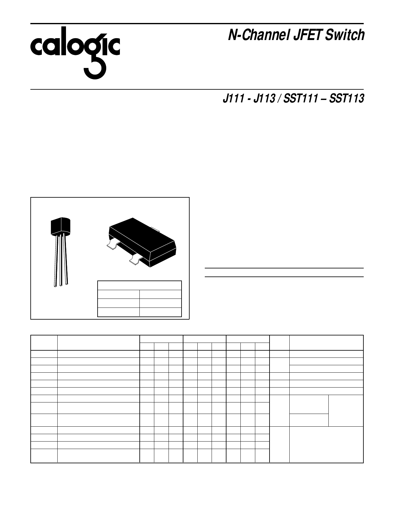
PIN CONFIGURATION
SOT-23
G
TO-92
D
S
D SG
5001
PRODUCT MARKING (SOT-23)
SST111
111
SST112
112
SST113
113
APPLICATIONS
Analog Switches
• Choppers
•• Commutators
ABSOLUTE MAXIMUM RATINGS
(TA = 25oC unless otherwise specified)
Gate-Drain or Gate-Source Voltage . . . . . . . . . . . . . . . . -35V
Gate Current . . . . . . . . . . . . . . . . . . . . . . . . . . . . . . . . . 50mA
Storage Temperature Range . . . . . . . . . . . . . -55oC to +150oC
Operating Temperature Range . . . . . . . . . . . -55oC to +135oC
Lead Temperature (Soldering, 10sec) . . . . . . . . . . . . . +300oC
Power Dissipation . . . . . . . . . . . . . . . . . . . . . . . . . . . 360mW
Derate above 25oC . . . . . . . . . . . . . . . . . . . . . . 3.3mW/oC
NOTE: Stresses above those listed under "Absolute Maximum
Ratings" may cause permanent damage to the device. These are
stress ratings only and functional operation of the device at these or
any other conditions above those indicated in the operational sections
of the specifications is not implied. Exposure to absolute maximum
rating conditions for extended periods may affect device reliability.
ORDERING INFORMATION
Part
Package
Temperature Range
J111-113 Plastic SOT-23
SST111-113 Plastic SOT-23
-55oC to +135oC
-55oC to +135oC
For Sorted Chips in Carriers see 2N4391 series.
ELECTRICAL CHARACTERISTICS (TA = 25oC unless otherwise specified)
SYMBOL
IGSSR
VGS(off)
BVGSS
IDSS
ID(off)
rDS(on)
Cdg(off)
Csg(off)
Cdg(on)
+ Csg(on)
td(on)
tr
td(off)
tf
PARAMETER
Gate Reverse Current (Note 1)
Gate Source Cutoff Voltage
Gate Source Breakdown Voltage
Drain Saturation Current (Note 2)
Drain Cutoff Current (Note 1)
Drain Source ON Resistance
Drain Gate OFF Capacitance
Source Gate OFF Capacitance
Drain Gate Plus Source Gate ON
Capacitance
Turn On Delay Time
Rise Time
Turn Off Delay Time
Fall Time
111
112
113
UNITS
MIN TYP MAX MIN TYP MAX MIN TYP MAX
-1
-1
-1 nA
-3
-10 -1
-35
-35
-5 -0.5
-35
-3
V
20
5
2
mA
1
1
1 nA
30
50
100 Ω
5
5
5
5
5
5
pF
28
28
28
7
7
7
6
6
6
20
20
20
ns
15
15
15
TEST CONDITIONS
VDS = 0V, VGS = -15V
VDS = 5V, ID = 1µA
VDS = 0V, IG = -1µA
VDS = 15V, VGS = 0V
VDS = 5V, VGS = -10V
VDS = 0.1V, VGS = 0V
VDS = 0,
VGS = -10V
(Note 3)
f = 1MHz
VDS = VGS = 0
(Note 3)
Switching Time Test
Conditions (Note 3)
J111 J112
VDD 10V 10V
VGS(off) -12V -7V
RL 0.8kΩ 1.6kΩ
J113
10V
-5V
3.2kΩ
NOTES: 1. Approximately doubles for every 10oC increase in TA.
2. Pulse test duration 300µs; duty cycle ≤3%.
3. For design reference only, not 100% tested.
CALOGIC CORPORATION, 237 Whitney Place, Fremont, California 94539, Telephone: 510-656-2900, FAX: 510-651-1076
Share Link: 