DS1742W-120 查看數據表(PDF) - Dallas Semiconductor -> Maxim Integrated
零件编号
产品描述 (功能)
生产厂家
DS1742W-120 Datasheet PDF : 12 Pages
| |||
DS1742
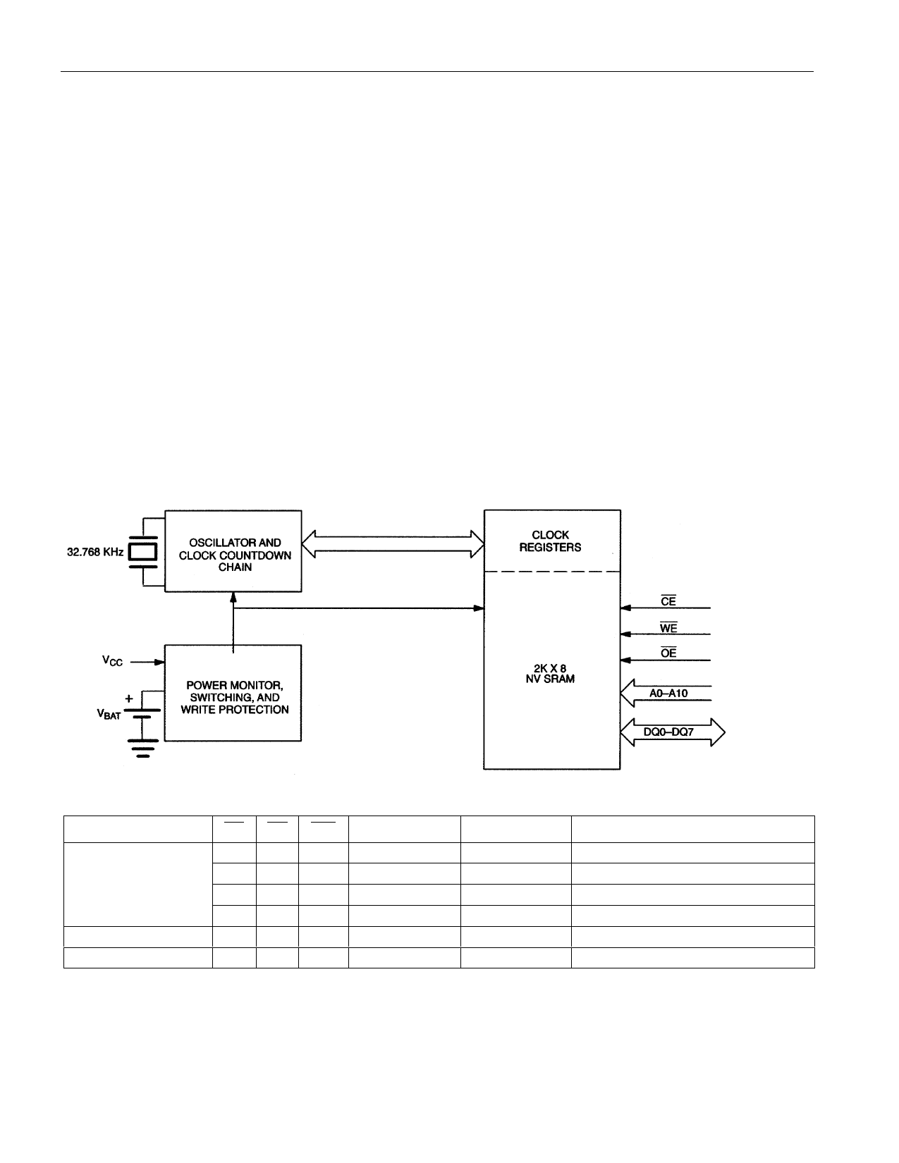
The RTC clock registers are double-buffered to avoid access of incorrect data that can occur during clock
update cycles. The double buffered system also prevents time loss as the timekeeping countdown
continues unabated by access to time register data. The DS1742 also contains its own power-fail
circuitry, which deselects the device when the VCC supply is in an out of tolerance condition. This feature
prevents loss of data from unpredictable system operation brought on by low VCC as errant access and
update cycles are avoided.
CLOCK OPERATIONS-READING THE CLOCK
While the double-buffered register structure reduces the chance of reading incorrect data, internal updates
to the DS1742 clock registers should be halted before clock data is read to prevent reading of data in
transition. However, halting the internal clock register updating process does not affect clock accuracy.
Updating is halted when a 1 is written into the read bit, bit 6 of the century register, see Table 2. As long
as a 1 remains in that position, updating is halted. After a halt is issued, the registers reflect the count,
that is day, date, and time that was current at the moment the halt command was issued. However, the
internal clock registers of the double-buffered system continue to update so that the clock accuracy is not
affected by the access of data. All of the DS1742 registers are updated simultaneously after the internal
clock register updating process has been re-enabled. Updating is within a second after the read bit is
written to 0. The READ bit must be a zero for a minimum of 500 µs to ensure the external registers will
be updated.
DS1742 BLOCK DIAGRAM Figure 1
DS1742 TRUTH TABLE Table 1
VCC
VCC>VPF
VSO<VCC<VPF
VCC<VSO<VPF
CE OE WE
VIH X X
VIL X VIL
VIL VIL VIH
VIL VIH VIH
XX X
XX X
MODE
DESELECT
WRITE
READ
READ
DESELECT
DESELECT
DQ
HIGH-Z
DATA IN
DATA OUT
HIGH-Z
HIGH-Z
HIGH-Z
POWER
STANDBY
ACTIVE
ACTIVE
ACTIVE
CMOS STANDBY
DATA RETENTION MODE
SETTING THE CLOCK
As shown in Table 2, bit 7 of the century register is the write bit. Setting the write bit to a 1, like the read
bit, halts updates to the DS1742 registers. The user can then load them with the correct day, date and
time data in 24-hour BCD format. Resetting the write bit to a 0 then transfers those values to the actual
clock counters and allows normal operation to resume.
2 of 12
Share Link: 