DS1742W-120 查看數據表(PDF) - Dallas Semiconductor -> Maxim Integrated
零件编号
产品描述 (功能)
生产厂家
DS1742W-120 Datasheet PDF : 12 Pages
| |||
DS1742
STOPPING AND STARTING THE CLOCK OSCILLATOR
The clock oscillator may be stopped at any time. To increase the shelf life, the oscillator can be turned
off to minimize current drain from the battery. The OSC bit is the MSB (bit 7) of the seconds registers,
see Table 2. Setting it to a 1 stops the oscillator.
FREQUENCY TEST BIT
As shown in Table 2, bit 6 of the day byte is the frequency test bit. When the frequency test bit is set to
logic 1 and the oscillator is running, the LSB of the seconds register will toggle at 512 Hz. When the
seconds register is being read, the DQ0 line will toggle at the 512 Hz frequency as long as conditions for
access remain valid (i.e., CE low, OE low, WE high, and address for seconds register remain valid and
stable).
CLOCK ACCURACY
The DS1742 is guaranteed to keep time accuracy to within ±1 minute per month at 25°C. The RTC is
calibrated at the factory by Dallas Semiconductor using nonvolatile tuning elements. The DS1742 does
not require additional calibration. For this reason, methods of field clock calibration are not available and
not necessary. Clock accuracy is also effected by the electrical environment and caution should be taken
to place the RTC in the lowest level EMI section of the PCB layout. For additional information please
see application note 58.
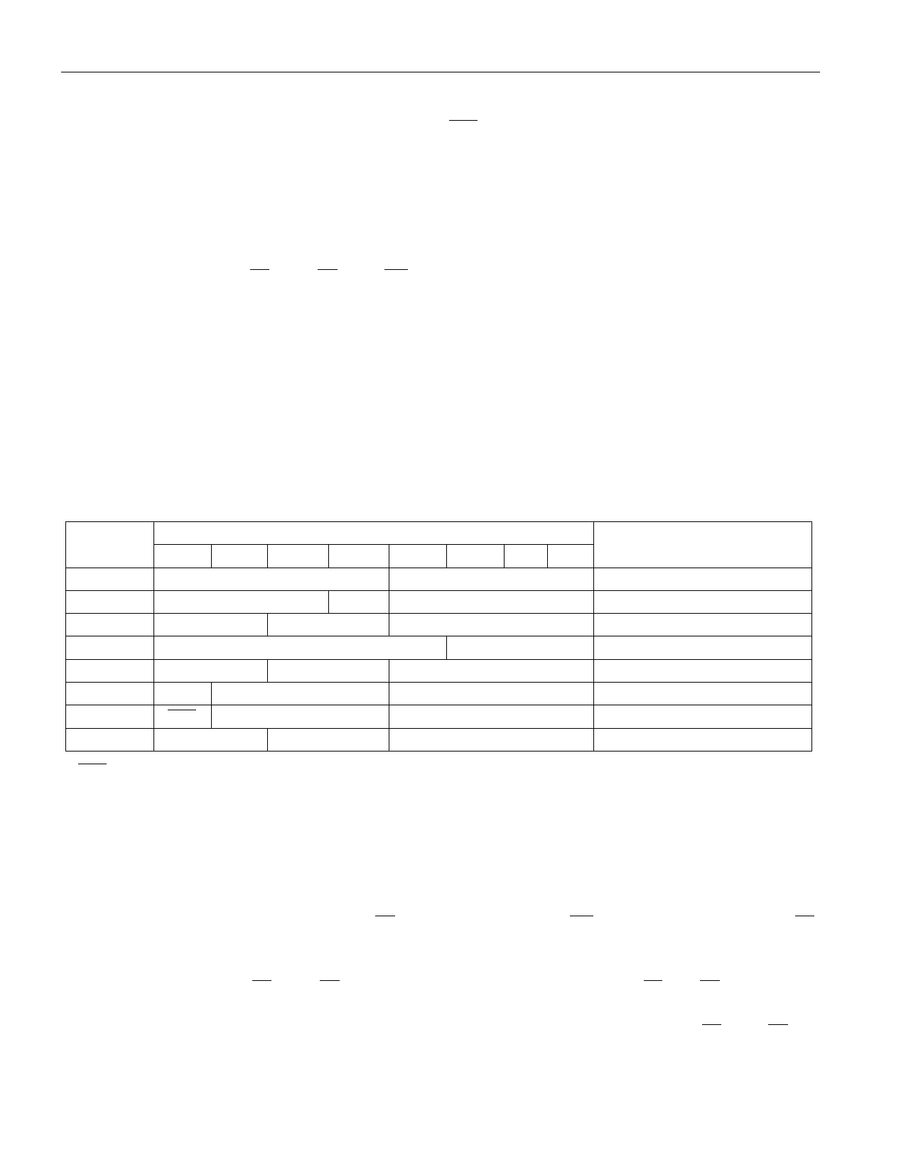
DS1742 REGISTER MAP Table 2
ADDRESS
B7
7FF
B6
B5
10 Year
DATA
B4
B3
7FE
X
X
X 10 Mo
7FD
X
X
10 Date
7FC
BF
FT
X
X
X
7FB
X
X
10 HOUR
7FA
X
10 MINUTES
7F9
OSC
10 SECONDS
7F8
W
R
10 CENTURY
B2
B1
YEAR
MONTH
DATE
DAY
HOUR
MINUTES
SECONDS
CENTURY
OSC = STOP BIT
W = WRITE BIT
R = READ BIT
X = SEE NOTE BELOW
FUNCTION/RANGE
B0
YEAR
00-99
MONTH
01-12
DATE
01-31
DAY
01-07
HOUR
00-23
MINUTES
00-59
SECONDS
00-59
CONTROL
00-39
FT = FREQUENCY TEST
BF = BATTERY FLAG
NOTE:
All indicated “X” bits are not dedicated to any particular function and can be used as normal RAM bits.
RETRIEVING DATA FROM RAM OR CLOCK
The DS1742 is in the read mode whenever OE (output enable) is low, WE (write enable) is high, and CE
(chip enable) is low. The device architecture allows ripplethrough access to any of the address locations
in the NV SRAM. Valid data will be available at the DQ pins within tAA after the last address input is
stable, providing that the CE , and OE access times and states are satisfied. If CE , or OE access times
and states are not met, valid data will be available at the latter of chip enable access (tCEA) or at output
enable access time (tOEA). The state of the data input/output pins (DQ) is controlled by CE , and OE . If
the outputs are activated before tAA, the data lines are driven to an intermediate state until tAA. If the
3 of 12
Share Link: 