LA4534M 查看數據表(PDF) - SANYO -> Panasonic
零件编号
产品描述 (功能)
生产厂家
LA4534M Datasheet PDF : 9 Pages
| |||
LA4534M
Operating Characteristics at Ta = 25˚C, RL=16Ω, Rg=600Ω
Parameter
Symbol
Conditions
Ratings
Unit
min typ max
Quiescent current
Voltage gain
Voltage gain variations
Total harmonic distortion
Output power
Crosstalk
Ripple rejection
Output noise voltage
ICCO1
ICCO2
ICCO3
VG1
VG2
∆VG1
∆VG2
THD
PO
CT
SVRR
VNO
VCC=2.4V, Quiescent time
VCC=4.5V, pin 10 to GND
VCC=4.5V, pin 1 to GND
VCC=2.4V, f=1kHz, VO=–10dBm
VCC=1.6V, f=1kHz, VO=–20dBm
VCC=2.4V, f=1kHz, VO=–10dBm
VCC=1.6V, f=1kHz, VO=–20dBm
VCC=2.0V, f=1kHz, PO=1mW
VCC=3.0V, f=1kHz, THD=10%
VCC=2.4V, f=1kHz, Rg=1kΩ,
VO=–10dBm
VCC=1.6V, f=100Hz, Rg=1kΩ,
VR=–20dBm, BPF=100Hz
VCC=4.5V, Rg=1kΩ,
BPF=20Hz to 20kHz
5.4
10 mA
1.1
2.0 mA
1.0 µA
9
11
13 dB
9
11
13 dB
1.0 dB
1.0 dB
0.08 0.24 %
25
50
mW
40
50
mW
50
70
dB
7
20 µV
Power off effect
Mute effect
Power on current sensitivity
Power off voltage sensitivity
Mute off current sensitivity
Mute on voltage sensitivity
VO(off)
VO(MT)
I1(on)
V1(off)
I10(off)
V10(on)
VCC=1.6V, f=100Hz, Pin 1 to GND,
VIN=–10dBm
VCC=1.6V, f=100Hz, Pin 10 to GND,
VIN=–10dBm
VCC=1.5V, V5≥0.85V
VCC=1.5V, V5≤0.1V
VCC=1.5V, V5≥0.85V
VCC=1.5V, V5≤0.1V
0.05
0.5
0.6
0.2
0.5 0.65
–80 dBm
–80 dBm
1.0 µA
V
1.0 µA
V
Note : Quiescent current is the current flowing into pin 6. The current flowing into pin 1 and pin 10 is at the maximum value and calculated from
the equation (V pin–0.5V)/16[V/kΩ], increasing total current.
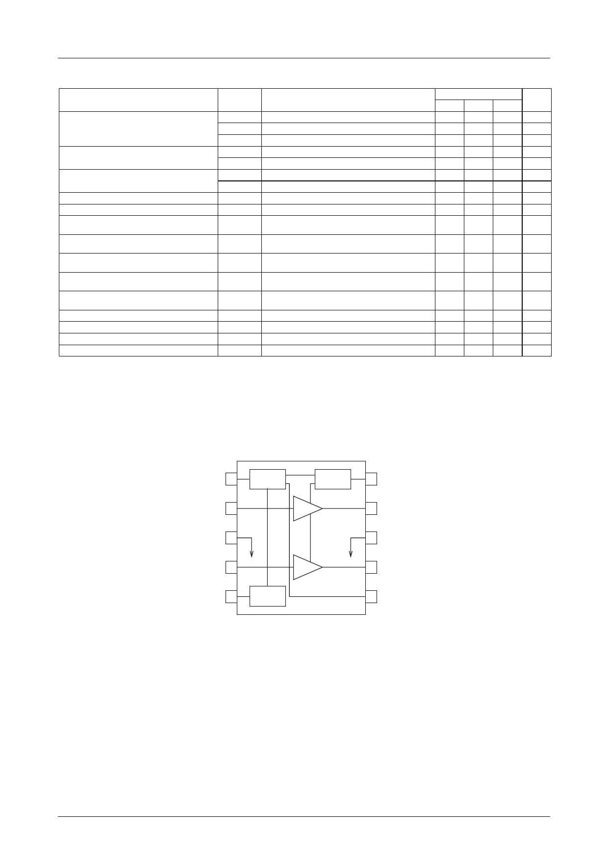
Equivalent Circuit Block Diagram
P/SW 1
IN 1 2
POWER
SWITCH
MUTE
CIRCUIT
Amp1
10 MT/SW
9 OUT 1
PRE GND 3
8 POWER GND
IN 2 4
Amp2
7 OUT 2
REF 5
BIAS
6 VCC
A11151
No.4024–2/9
Share Link: 