EDE1108AASE 查看數據表(PDF) - Elpida Memory, Inc
零件编号
产品描述 (功能)
生产厂家
EDE1108AASE Datasheet PDF : 65 Pages
| |||
EDE1104AASE, EDE1108AASE
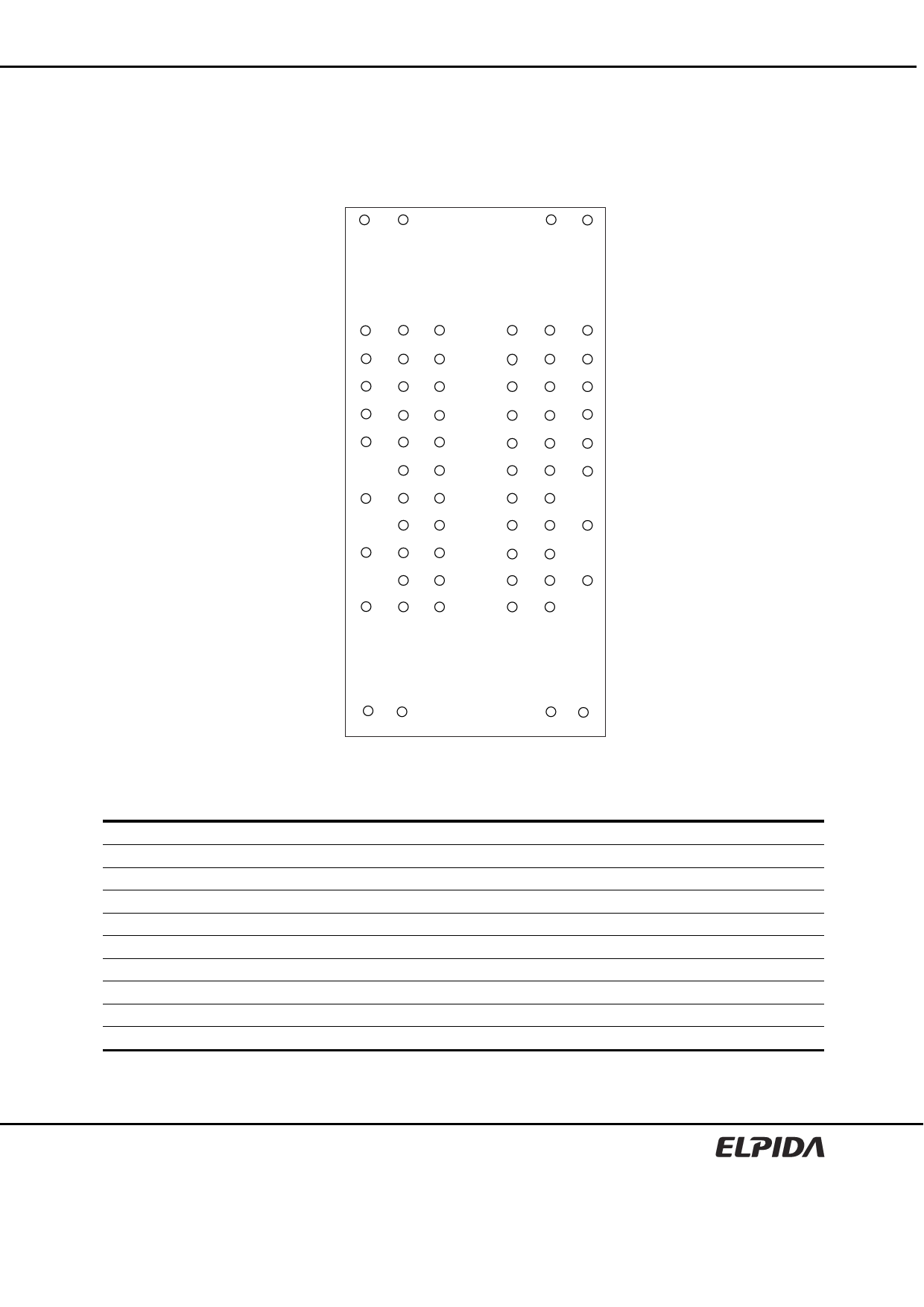
Pin Configurations
/xxx indicates active low signal.
68-ball FBGA (µBGA)
(×8, ×4 organization)
1
2
3
7
8
9
A
NC NC
B
NC NC
C
D
E
VDD NU/ /RDQS VSS
(NC)*
F
DQ6
(NC)*
VSSQ DM/RDQS
(DM)*
G
VDDQ DQ1 VDDQ
H
DQ4
(NC)*
VSSQ
DQ3
J
VDDL VREF VSS
K
CKE /WE
L
BA2 BA0 BA1
M
A10 A1
N
VSS A3 A5
P
A7 A9
R
VDD A12 NC
T
U
V
W
NC NC
VSSQ /DQS VDDQ
DQS
VSSQ
DQ7
(NC)*
VDDQ DQ0 VDDQ
DQ2
VSSQ
DQ5
(NC)*
VSSDL CK VDD
/RAS /CK ODT
/CAS /CS
A2 A0 VDD
A6 A4
A11 A8 VSS
NC A13
NC NC
(Top view)
Note: ( )* marked pins are for ×4 organization.
Pin name
Function
A0 to A13
Address inputs
BA0, BA1, BA2
Bank select
DQ0 to DQ7
Data input/output
DQS, /DQS
Differential data strobe
RDQS, /RDQS
Differential data strobe for read
/CS
Chip select
/RAS, /CAS, /WE
Command input
CKE
Clock enable
CK, /CK
Differential clock input
DM
Write data mask
Notes: 1. Not internally connected with die.
2. Don’t use other than reserved functions.
Pin name
ODT
VDD
VSS
VDDQ
VSSQ
VREF
VDDL
VSSDL
NC*1
NU*2
Function
ODT control
Supply voltage for internal circuit
Ground for internal circuit
Supply voltage for DQ circuit
Ground for DQ circuit
Input reference voltage
Supply voltage for DLL circuit
Ground for DLL circuit
No connection
Not usable
Data Sheet E0404E20 (Ver. 2.0)
3
Share Link: 