EDE1116AJBG-1 查看數據表(PDF) - Elpida Memory, Inc
零件编号
产品描述 (功能)
生产厂家
EDE1116AJBG-1 Datasheet PDF : 74 Pages
| |||
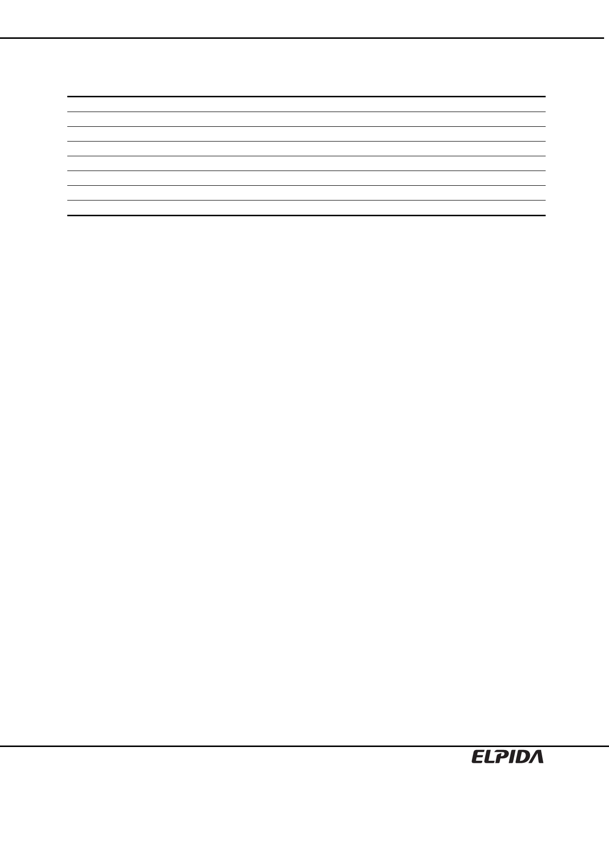
EDE1108AJBG-1, EDE1116AJBG-1
Recommended DC Operating Conditions (SSTL_18)
Parameter
Symbol
min.
typ.
max.
Unit
Notes
Supply voltage
VDD
1.7
1.8
1.9
V
4
Supply voltage for output
VDDQ
1.7
1.8
1.9
V
4
Input reference voltage
VREF
0.49 × VDDQ
0.50 × VDDQ 0.51 × VDDQ
V
1, 2
Termination voltage
VTT
VREF − 0.04
VREF
VREF + 0.04
V
3
DC input logic high
VIH (DC)
VREF + 0.125
VDDQ + 0.3
V
DC input logic low
VIL (DC)
−0.3
VREF – 0.125 V
AC input logic high
VIH (AC)
VREF + 0.200
V
AC input logic low
VIL (AC)
VREF − 0.200 V
Notes: 1. The value of VREF may be selected by the user to provide optimum noise margin in the system. Typically
the value of VREF is expected to be about 0.5 × VDDQ of the transmitting device and VREF are expected
to track variations in VDDQ.
2. Peak to peak AC noise on VREF may not exceed ±2% VREF (DC).
3. VTT of transmitting device must track VREF of receiving device.
4. VDDQ tracks with VDD, VDDL tracks with VDD. AC parameters are measured with VDD, VDDQ and
VDDL tied together.
Data Sheet E1733E31 (Ver.3.1)
6
Share Link: 