EDE1108AJBG-1 查看數據表(PDF) - Elpida Memory, Inc
零件编号
产品描述 (功能)
生产厂家
EDE1108AJBG-1 Datasheet PDF : 74 Pages
| |||
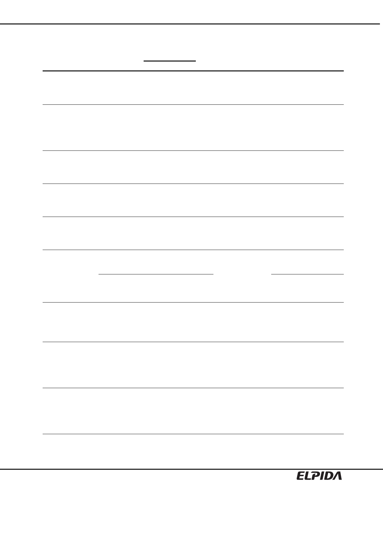
EDE1108AJBG-1, EDE1116AJBG-1
DC Characteristics 1 (TC = 0°C to +85°C, VDD, VDDQ = 1.8V ± 0.1V)
Parameter
Operating current
(ACT-PRE)
max.
Symbol Grade × 8
× 16
IDD0
50
60
Operating current
(ACT-READ-PRE)
IDD1
60
80
Precharge power-down
standby current
IDD2P
Precharge quiet
standby current
IDD2Q
10
10
20
20
Idle standby current IDD2N
25
25
Active power-down
standby current
IDD3P-F
IDD3P-S
27
27
15
15
Active standby current IDD3N
45
45
Operating current
(Burst read operating)
IDD4R
110
130
Operating current
(Burst write operating)
IDD4W
115
140
Unit Test condition
one bank; tCK = tCK (IDD), tRC = tRC (IDD),
tRAS = tRAS min.(IDD);
mA CKE is H, /CS is H between valid commands;
Address bus inputs are SWITCHING;
Data bus inputs are SWITCHING
one bank; IOUT = 0mA;
BL = 4, CL = CL(IDD), AL = 0;
tCK = tCK (IDD), tRC = tRC (IDD),
mA tRAS = tRAS min.(IDD); tRCD = tRCD (IDD);
CKE is H, /CS is H between valid commands;
Address bus inputs are SWITCHING;
Data pattern is same as IDD4W
all banks idle;
tCK = tCK (IDD);
mA CKE is L;
Other control and address bus inputs are STABLE;
Data bus inputs are FLOATING
all banks idle;
tCK = tCK (IDD);
mA CKE is H, /CS is H;
Other control and address bus inputs are STABLE;
Data bus inputs are FLOATING
all banks idle;
tCK = tCK (IDD);
mA CKE is H, /CS is H;
Other control and address bus inputs are SWITCHING;
Data bus inputs are SWITCHING
all banks open;
mA tCK = tCK (IDD);
CKE is L;
Fast PDN Exit
MRS (12) = 0
Other control and
address bus inputs are
mA STABLE;
Data bus inputs are
Slow PDN Exit
MRS (12) = 1
FLOATING
all banks open;
tCK = tCK (IDD), tRAS = tRAS max.(IDD), tRP = tRP
mA
(IDD);
CKE is H, /CS is H between valid commands;
Other control and address bus inputs are SWITCHING;
Data bus inputs are SWITCHING
all banks open, continuous burst reads, IOUT = 0mA;
BL = 4, CL = CL(IDD), AL = 0;
tCK = tCK (IDD), tRAS = tRAS max.(IDD),
mA tRP = tRP (IDD);
CKE is H, /CS is H between valid commands;
Address bus inputs are SWITCHING;
Data pattern is same as IDD4W
all banks open, continuous burst writes;
BL = 4, CL = CL(IDD), AL = 0;
tCK = tCK (IDD), tRAS = tRAS max.(IDD),
mA tRP = tRP (IDD);
CKE is H, /CS is H between valid commands;
Address bus inputs are SWITCHING;
Data bus inputs are SWITCHING
Data Sheet E1733E31 (Ver.3.1)
8
Share Link: 