EDI2DL32256V 查看數據表(PDF) - White Electronic Designs Corporation
零件编号
产品描述 (功能)
生产厂家
EDI2DL32256V Datasheet PDF : 8 Pages
| |||
EDI2DL32256V
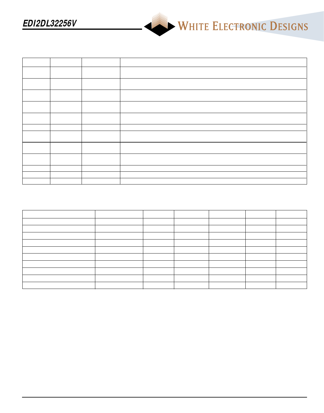
Pin
Various
L5,G5
G3,L3
M4
K4
E4
F4
B4
R3
T7
Various
Various
Various
Symbol
A0-17
BE0\,BE1\,
BE2\,BE3\
BWE\
CLK
CE\
OE\
ADSC\
MODE
ZZ
DQ0-31
Vcc
Vss
Type
Input
Synchronous
Input
Synchronous
Input
Synchronous
Input
Synchronous
Input
Synchronous
Input
Input
Synchronous
Input
Input
Synchronous
Input/Output
Supply
Ground
PIN DESCRIPTIONS
Description
Addresses: These inputs are registered and must meet setup and hold times around the rising edge
of CLK.
Byte Write: A byte write is LOW for a WRITE cycle and HIGH for a READ BE2\, BE3\ cycle. BE0\ controls
DQ0-7. BE1\ controls DQ8-15. BE2\ controls DQ16-23. BE3\ controls DQ24-31
Byte Write Enable: This active LOW input gates byte write operations and must meet the setup and hold
times around the rising edge of CLK.
Clock:This signal registers the addresses, data, chip enables, write control and burst control inputs on
its rising edge. All synchronous inputs must meet setup and hold times around the clockís rising edge.
Chip Enable: This active LOW inputs is used to enable the device.
Output Enable: This active LOW asynchronous input enables the data output drivers
Address Status Controller: This active LOW input causes device to be deselected or selected along with new
external address to be registered. A READ or WRITE cycle is initiated depending upon write control inputs.
Static Mode: This input selects the burst sequence. A LOW on this pin selects LINEAR BURST. A NC or
HIGH on this pin selects INTERLEAVED BURST.
Snooze: This active HIGH input puts the device in low power consumption standby mode. For normal
operation, this input has to be either LOW or NC (no connect)
Data Inputs/Outputs: First byte is DQ0-7, second byte is DQ8-15, third byte is DQ16-23, fourth byte is DQ24-31
Core power supply: +3.3V -5%/+5%
Ground
TRUTH TABLE
Operation
Address Used
CE\
ADSC\
WRITE\
Deselected Cycle, Power Down
None
H
L
X
WRITE Cycle, Begin Burst
External
L
L
L
READ Cycle, Begin Burst
External
L
L
H
READ Cycle, Begin Burst
External
L
L
H
READ Cycle, Suspend Burst
Current
X
H
H
READ Cycle, Suspend Burst
Current
X
H
H
READ Cycle, Suspend Burst
Current
H
H
H
READ Cycle, Suspend Burst
Current
H
H
H
WRITE Cycle, Suspend Burst
Current
X
H
L
WRITE Cycle, Suspend Burst
Current
H
H
L
OE\
DQ
X
High-Z
X
D
L
Q
H
High-Z
L
Q
H
High-Z
L
Q
H
High-Z
X
D
X
D
NOTE:
1. X means ìdonít careî, H means logic HIGH. L means logic LOW.
2a.WRITE\ = L, means [BE0\*BE1\*BE2\*BE3\]*BWE\ equals LOW
2b.WRITE\ = H, means [BE0\*BE1\*BE2\*BE3\]*BWE\ equals HIGH
3. All inputs except OE\ must meet setup and hold times around the rising edge (LOW to HIGH) of CLK.
4. Suspending burst generates wait cycle
5. For a write operation following a read operation, OE\ must be HIGH before the input data required setup time plus High-Z time for OE\ and staying HIGH though
out the input data hold time.
6. This device contains circuitry that will ensure the outputs will be in High-Z during power-up.
White Electronic Designs Corporation • (508) 366-5151 • www.whiteedc.com
2
November 2000, Rev. 1
ECO #13417
Share Link: 