TQ5622 查看數據表(PDF) - TriQuint Semiconductor
零件编号
产品描述 (功能)
生产厂家
TQ5622 Datasheet PDF : 9 Pages
| |||
TQ5622 Product Description
The TQ5622 3V RFIC Downconverter is designed specifically
for PCS band TDMA applications. The TQ5622 contains LNA,
Mixer and LO buffer circuits matched to the 1900 MHz US PCS
frequency band. Any IF frequency may be selected between 85
and 150 MHz. Most RF ports are internally matched to 50 Ω
simplifying the design and minimizing the number of external
components. The TQ5622 also includes a power–down mode
switch which allows current saving during standby and the non-
operating portion of the TDMA pulse.
Operation
Please refer to the test circuit above.
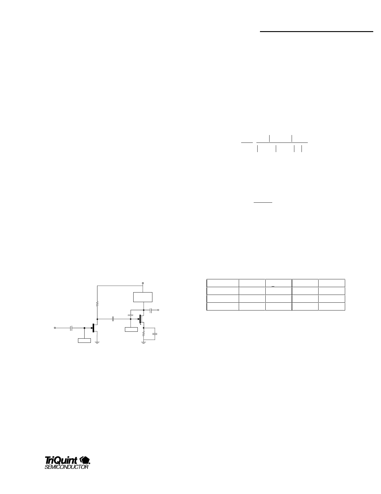
Low Noise Amplifier (LNA)
The LNA section of the TQ5622 are cascaded common source
FET’s, see Figure 1. It is designed to operate on DC supply
voltages from 2.7V to 5V. The source terminal must be
grounded as close as possible to Pin 1 to avoid significant gain
reduction due to degeneration. The LNA requires an input
matching circuit to obtain best noise figure, gain and return loss.
The LNA output is close to 50 Ω for direct connection to a 50 Ω
image reject filter.
Vdd
LNA
in
BIAS
LOAD
LNA
out
BIAS
Figure 1. Simplified Schematic of LNA Section
LNA Input Match
The designer can make some Noise Figure and Gain trade off
by varying the off chip LNA input matching circuit values and
topology. This allows the TQ5622 to be optimized for specific
system requirements.
The LNA gain, noise figure and input return loss are a function
of the source impedance (Zs), or reflection coefficient (Γs),
TQ5622
Data Sheet
presented to the input pin. Highest gain and lowest return loss
occur when Γs is equal to the complex conjugate of the LNA
input impedance. A different source reflection coefficient, Γopt,
which is experimentally determined, will provide the lowest noise
figure, Fmin.
The noise resistance, Rn, provides an indication of the sensitivity
of the noise performance to changes in Γs as seen by the LNA
input.
( ) FLNA
=
FMIN
+
4 RN
Z0
⋅
1+
Γopt
Γ2
opt
− ΓS 2
⋅ 1 − Γs
2
Components such as filters and mixers placed after the LNA
degrade the overall system noise figure according to the
following equation:
FSYSTEM = FLNA + F2 − 1
GLNA
FLNA and GLNA represent the linear noise factor and gain of the
LNA and F2 is the noise factor of the next stage. The system
noise figure is a compromise between the highest gain and
minimum noise figure of the LNA. See Table 1 for noise
parameters.
Table 1. TQ5622 Noise Parameters
Freq. MHz |Gopt| / Gopt Fmin
Rn
1930
0.70
97
1.2
17
1960
0.70
94
1.2
18
1990
0.69
91
1.2
19
LNA Output Match
The output impedance of the LNA was designed for 50Ω. The
internal 50Ω match eliminates the need for external
components at this port. It also improves IP3 performance and
power gain.
The output of the LNA is intended to be connected directly to an
image reject filter. Depending on the filter, additional
components may be needed to better match to the LNA output.
Some image reject filters may require a series inductor to
smooth the frequency response and improve overall
performance.
For additional information and latest specifications, see our website: www.triquint.com
5
Share Link: 