TQ5622 查看數據表(PDF) - TriQuint Semiconductor
零件编号
产品描述 (功能)
生产厂家
TQ5622 Datasheet PDF : 9 Pages
| |||
TQ5622
Data Sheet
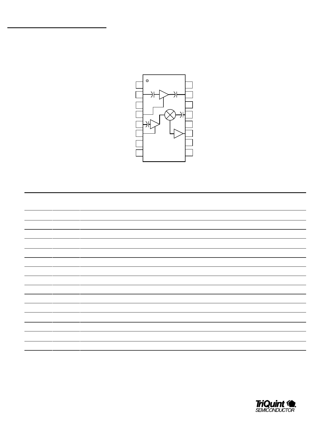
Package Pinout
GND 1
RF IN 2
GND 3
VDD LNA 4
LO IN 5
Vdd MXR 6
GND 7
GND 8
16 Sleep
Control
15 LNA Out
14 GND
13 MXR RF IN
12 GND
11 IF OUT/Vdd
10 GND
9 GND
Pin Descriptions
Pin Name
GND, LNA
Pin # Description and Usage
1
LNA first stage ground connection. Direct connection to ground required.
LNA IN
2
LNA RF input. DC blocked. Requires external matching elements for noise match and match to 50Ω
GND
3
Ground
VDD LNA
4
LNA DC supply voltage. Local external bypass capacitor required.
MXR LO IN
5
Mixer LO input. DC blocked, matched to 50Ω
VDD_MXR
6
Mixer LO buffer supply voltage. Local external bypass capacitor required.
GND
7
Ground
GND
8
Ground
GND
9
Ground
GND
10
Ground
IF OUT
11
IF output. Open drain output, connection to Vdd required. External matching is required.
GND
12
Ground
MXR_RF
13
Mixer RF input, DC blocked. Matched to 50Ω.
GND
14
Ground
LNA OUT
15
LNA RF Output. DC blocked. Matched to 50Ω.
SLEEP
16
Power-Down mode control.
For ground pins 1,3,7,8,9,10,12, and 14, TriQuint recommends use of several via holes to the backside ground immediately adjacent to the
pin.
Package Type: Power QSOP-16 Plastic Package
8
For additional information and latest specifications, see our website: www.triquint.com
Share Link: 