UPC2756TB 查看數據表(PDF) - NEC => Renesas Technology
零件编号
产品描述 (功能)
生产厂家
UPC2756TB
NEC => Renesas Technology

UPC2756TB Datasheet PDF : 16 Pages
| |||
µPC2756TB
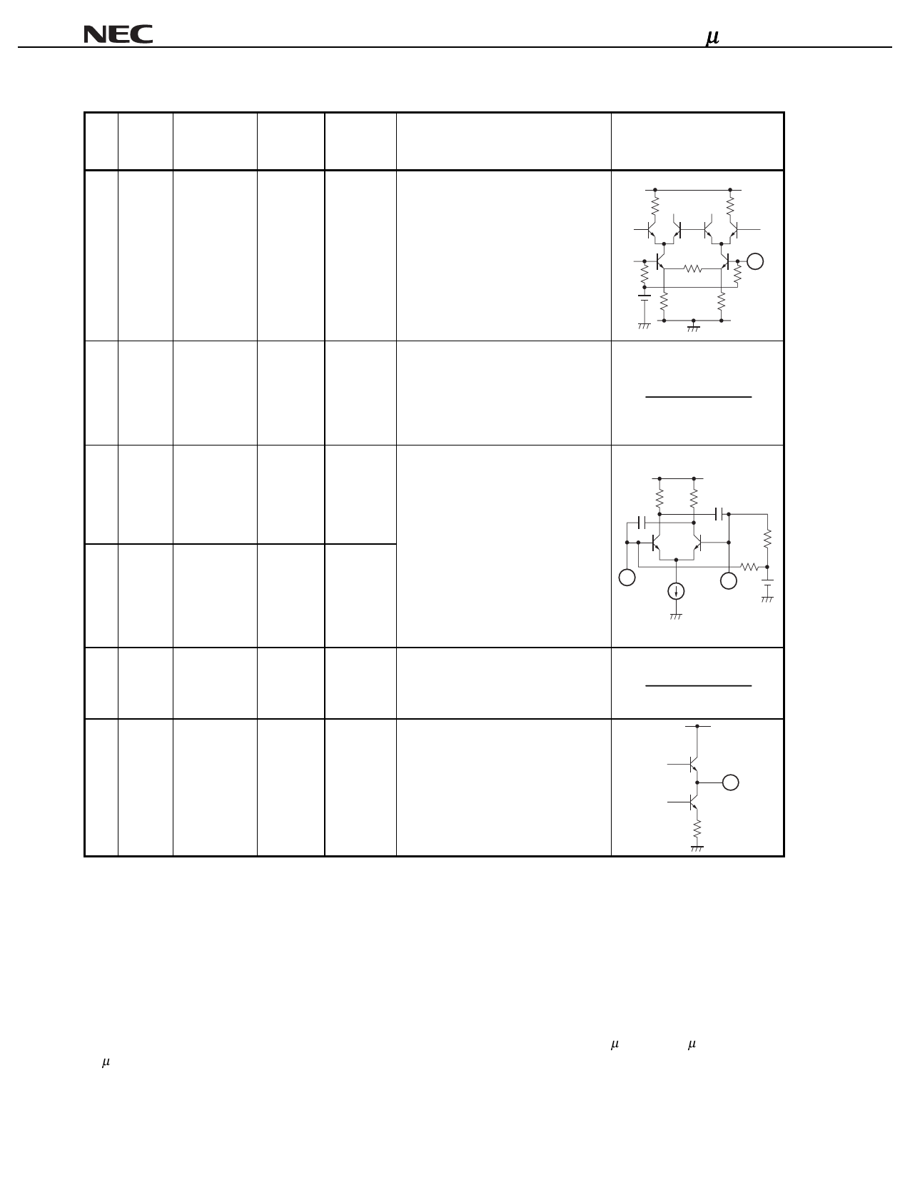
PIN EXPLANATION
Pin
Symbol Assignment
No.
1
RFin
RF input
Applied
Voltage
V
–
2 GND
Ground
0
3
LO1 Local oscillator
–
base collector
4
LO2 Local oscillator
–
base collector
5
VCC Power supply 2.7 to 3.3
6 IF out
IF output
–
Pin
Voltage
VNote
Function and Application
Equivalent Circuit
1.2
This pin is RF input for mixer designed
VCC
as double balance type.
This circuit contributes to suppress
spurious signal with minimum LO and
bias power consumption.
Also this symmetrical circuit can keep
1
specified performance insensitive to
process-condition distribution.
This pin must be externally coupled to
front stage with capacitor for DC cut.
–
Must be connected to the system
ground with minimum inductance.
Ground pattern on the board should
be formed as wide as possible.
(Track length should be kept as short
as possible.)
1.2
These pins are both base-collector of
oscillator. This oscillator is designed
as differential amplifier type.
3 pin and 4 pin should be externally
equipped with tank resonator circuit in
order to oscillate with feedback loop.
1.2
Also this symmetrical circuit can keep
specified performance insensitive to
3
process-condition distribution.
Each pin must be externally coupled
to tank circuit with capacitor for DC
cut.
VCC
4
–
Supply voltage 3.0 ± 0.3 V for
operation. Must be connected bypass
capacitor (e.g. 1 000 pF) to minimize
ground impedance.
1.7
This pin is output from IF buffer
VCC
amplifier designed as single-ended
push-pull type.
This pin is assigned for emitter
6
follower output with low-impedance.
This pin must be externally coupled to
next stage with capacitor for DC cut.
Note Pin voltage is measured at VCC = 3.0 V
APPLICATION
This IC is guaranteed on the test circuit constructed with 50 Ω equipment and transmission line. This IC, however,
does not have 50 Ω input/output impedance, but electrical characteristics such as conversion gain and
intermodulation distortion are described herein on these conditions without impedance matching. So, you should
understand that conversion gain and intermodulation distortion at input level will vary when you improve VS of RF
input with external circuit (50 Ω termination or impedance matching).
External circuits of the IC are explained in a following application note.
• To RF and IF port : Application Note “Usage and Application Characteristics of µPC2757T, µPC2758T and
µPC8112T, 3-V Power Supply, 1.9-GHz Frequency Down Converter ICs for Cellular/Cordless Telephone and
Portable Wireless Communication” (Document No. P11997E)
4
Data Sheet P12807EJ2V0DS00
Share Link: