EL7564 查看數據表(PDF) - Intersil
零件编号
产品描述 (功能)
生产厂家
EL7564 Datasheet PDF : 17 Pages
| |||
EL7564
Absolute Maximum Ratings (TA = 25°C)
Supply Voltage between VIN or VDD and GND . . . . . . . . . . . . +6.5V
VLX Voltage . . . . . . . . . . . . . . . . . . . . . . . . . . . . . . . . . . . . VIN +0.3V
Input Voltage . . . . . . . . . . . . . . . . . . . . . . . . GND -0.3V, VDD +0.3V
VHI Voltage . . . . . . . . . . . . . . . . . . . . . . . . . . GND -0.3V, VLX +6.5V
Storage Temperature . . . . . . . . . . . . . . . . . . . . . . . .-65°C to +150°C
Operating Ambient Temperature . . . . . . . . . . . . . . . .-40°C to +85°C
Operating Junction Temperature . . . . . . . . . . . . . . . . . . . . . . . +135°
CAUTION: Stresses above those listed in “Absolute Maximum Ratings” may cause permanent damage to the device. This is a stress only rating and operation of the
device at these or any other conditions above those indicated in the operational sections of this specification is not implied.
IMPORTANT NOTE: All parameters having Min/Max specifications are guaranteed. Typical values are for information purposes only. Unless otherwise noted, all tests
are at the specified temperature and are pulsed tests, therefore: TJ = TC = TA
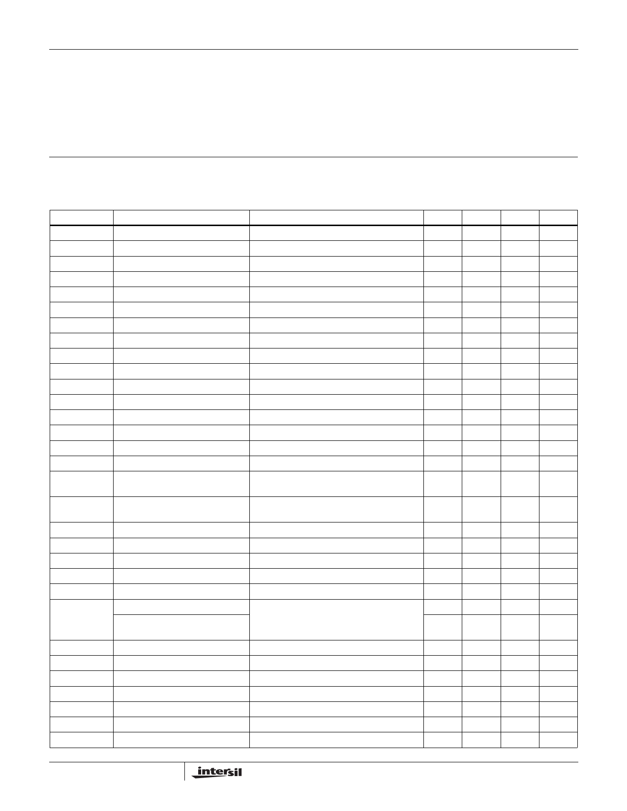
DC Electrical Specifications VDD = VIN = 5V, TA = TJ = 25°C, COSC = 1.2nF, Unless Otherwise Specified.
PARAMETER
DESCRIPTION
CONDITIONS
MIN
TYP
VREF
Reference Accuracy
1.24
1.26
VREFTC
Reference Temperature Coefficient
50
VREFLOAD
Reference Load Regulation
0 < IREF < 50µA
-1
VRAMP
Oscillator Ramp Amplitude
1.15
IOSC_CHG
Oscillator Charge Current
0.1V < VOSC < 1.25V
200
IOSC_DIS
Oscillator Discharge Current
0.1V < VOSC < 1.25V
8
IVDD+VDRV
VDD+VDRV Supply Current
VEN = 4V, FOSC = 120kHz
2
3.5
IVDD_OFF
VDD Standby Current
EN = 0
1
VDD_OFF
VDD for Shutdown
3.5
VDD_ON
VDD for Startup
4
TOT
Over Temperature Threshold
135
THYS
Over Temperature Hysteresis
20
ILEAK
Internal FET Leakage Current
EN = 0, LX = 5V (low FET), LX = 0V (high FET)
ILMAX
Peak Current Limit
5
RDSON
FET On Resistance
Wafer level test only
30
RDSONTC
RDSON Tempco
0.2
ISTP
Auxiliary Supply Tracking Positive VSTP = VIN / 2
Input Pull Down Current
-4
2.5
ISTN
Auxiliary Supply Tracking Negative VSTN = VIN / 2
2.5
Input Pull Up Current
VPGP
VPGN
VPG_HI
VPG_LO
VOVP
VFB
Positive Power Good Threshold
With respect to target output voltage
Negative Power Good Threshold With respect to target output voltage
Power Good Drive High
Power Good Drive Low
Over Voltage Protection
IPG = +1mA
IPG = -1mA
Output Initial Accuracy (EL7564CM) ILOAD = 0A
Output Initial Accuracy
(EL7564CRE)
6
-14
4
0.960
0.977
10
0.975
0.992
VFB_LINE
VFB_LOAD
VFB_TC
IFB
VEN_HI
VEN_LO
IEN
Output Line Regulation
Output Load Regulation
Output Temperature Stability
Feedback Input Pull Up Current
EN Input High Level
EN Input Low Level
Enable Pull Up Current
VIN = 5V, ∆VIN = 10%, ILOAD = 0A
0.5A < ILOAD < 4A
-40°C < TA < 85°C, ILOAD = 2A
VFB = 0V
VEN = 0
0.5
0.5
±1
100
3.2
1
-4
-2.5
MAX
1.28
5
1.5
3.9
4.35
10
60
UNIT
V
ppm/°C
%
V
µA
mA
mA
mA
V
V
°C
°C
µA
A
mΩ
mΩ/°C
µA
4
µA
14
%
-6
%
V
0.5
V
%
0.99
V
1.007
V
%
%
%
200
nA
4
V
V
µA
3
FN7297.3
May 9, 2005
Share Link: 