FAN5026(2011) 查看數據表(PDF) - Fairchild Semiconductor
零件编号
产品描述 (功能)
生产厂家
FAN5026 Datasheet PDF : 17 Pages
| |||
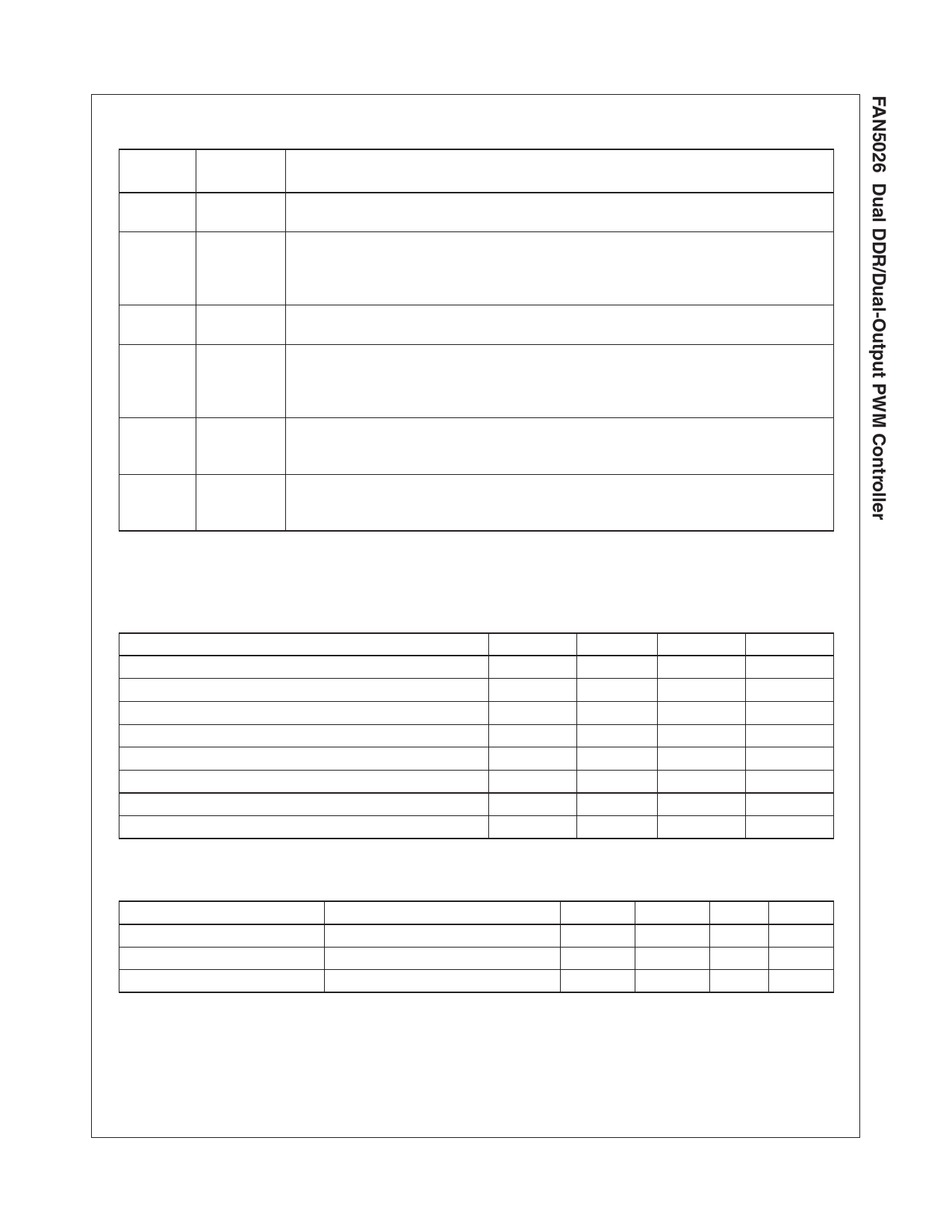
Pin Definitions
Pin # Name
Description
11
ILIM1 Current Limit 1. A resistor from this pin to GND sets the current limit.
12
SS1 Soft Start. A capacitor from this pin to GND programs the slew rate of the converter during
17
SS2 initialization. During initialization, this pin is charged with a 5mA current source.
13
DDR
DDR Mode Control. HIGH = DDR Mode. LOW = two separate regulators operating 180
degrees out of phase.
Input Voltage. Normally connected to the battery, providing voltage feedforward to set the
14
VIN
amplitude of the internal oscillator ramp. When using the IC for two-step conversion from 5V
input, connect through 100KΩ resistor to ground, which sets the appropriate ramp gain and
synchronizes the channels 90° out of phase.
15
PG1
Power-Good Flag. An open-drain output that pulls LOW when VSEN is outside a ±10% range of
the 0.9V reference.
Power-Good 2. When not in DDR Mode, open-drain output that pulls LOW when the VOUT is
16
PG2 / out of regulation or in a fault condition.
REF2OUT Reference Out 2. When in DDR Mode, provides a buffered output of REF2. Typically used as
the VDDQ/2 reference.
18
ILIM2 / Current Limit 2. When not in DDR Mode, a resistor from this pin to GND sets the current limit.
REF2 Reference for reg #2 when in DDR Mode. Typically set to VOUT1/2.
VCC. This pin powers the chip as well as the LDRV buffers. The IC starts to operate when
28
VCC voltage on this pin exceeds 4.6V (UVLO rising) and shuts down when it drops below 4.3V
(UVLO falling).
Block Diagram
© 2005 Fairchild Semiconductor Corporation
FAN5026 • Rev. 1.0.8
Figure 4. IC Block Diagram
4
www.fairchildsemi.com
Share Link: 