FAN7085 查看數據表(PDF) - Fairchild Semiconductor
零件编号
产品描述 (功能)
生产厂家
FAN7085 Datasheet PDF : 14 Pages
| |||
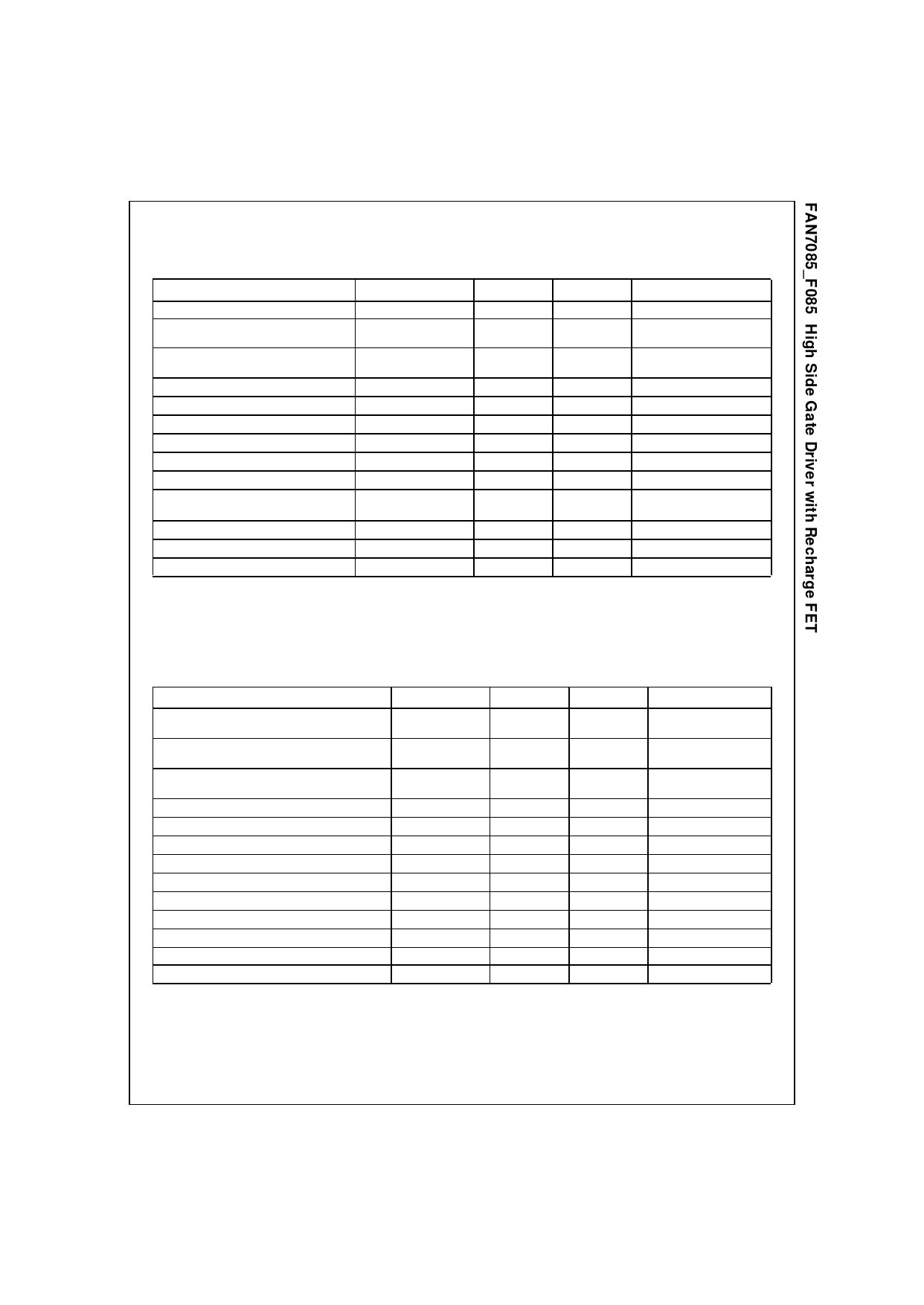
Absolute Maximum Ratings
Absolute Maximum Ratings indicate sustained limits beyond which damage to the device may occur. All voltage parameters are abso-
lute voltages referenced to GND.
Parameter
Symbol
Min.
Max.
Unit
High side floating supply voltage
High side driver output stage voltage
Neg. transient: 0.5 ms, external MOSFET off
High side floating supply offset voltage
Neg. transient 0.2 us
High side floating output voltage
Supply voltage
Input voltage for IN-
Input voltage for RESET-
Power Dissipation 1)
Thermal resistance, junction to ambient 1)
Electrostatic discharge voltage
(Human Body Model)
Charge device model
Junction Temperature
Storage Temperature
VBS
VB
Vs
VH O
VC C
VIN
VR E S
Pd
Rthja
VESD
VCDM
Tj
TS
-0.3
-5
-25
VS-0.3
-0.3
-0.3
-0.3
1.5K
500
-55
25
325
300
VB+0.3
25
Vcc+0.3
Vcc+0.3
0.625
200
150
150
V
V
V
V
V
V
V
W
°C/W
V
V
°C
°C
Note: 1) The thermal resistance and power dissipation rating are measured bellow conditions;
JESD51-2: Integrated Circuit Thermal Test Method Environmental Conditions - Natural condition(StillAir)
JESD51-3: Low Effective Thermal Conductivity Test Board for Leaded Surface Mount Package
Recommended Operating Conditions
For proper operation the device should be used within the recommended conditions.-40°C <= Ta <= 125°C
Parameter
High side floating supply voltage(DC)
Transient:-10V@ 0.2 us
High side floating supply offset voltage(DC)
@VBS=7V
High side floating supply offset voltage(Transient)
0.2us @VBS<25V
High side floating output voltage
Allowable offset voltage Slew Rate1)
Supply voltage for logic part
Input voltage for IN-
Input voltage for RESET-
Switching frequency 2)
Minimum low input width 3)
Minimum high input width 3)
Minimum operating voltage of VB related to GND
Ambient temperature
Symbol
VB
VS
VS
VH O
dv/dt
VCC
VI N
VR E S E T
Fs
tI N ( L o w , m i n )
tIN(high,min)
VB ( M I N )4)
Ta
Min.
VS+4.5
-3
-25
Vs
-
4.5
0
0
1000
60
4
-40
Max.
VS+20
300
300
VB
50
20
Vcc
Vcc
200K
-
-
-
125
Note: 1) Guaranteed by design.
2) Duty = 0.5, VBS >=7V
3) Guaranteed by design. Pulse widths below the specified values, may be ignored. Output will either follow the input signal or will ignore it.
No false output state is guaranteed when minimum input width is smaller than tin
4) Guaranteed by design
Unit
V
V
V
V
V/ns
V
V
V
Hz
ns
ns
V
°C
3
FAN7085_F085 Rev. 1.0.3
www.fairchildsemi.com
Share Link: 