FIN212AC(2008) 查看數據表(PDF) - Fairchild Semiconductor
零件编号
产品描述 (功能)
生产厂家
FIN212AC
(Rev.:2008)
(Rev.:2008)
Fairchild Semiconductor

FIN212AC Datasheet PDF : 23 Pages
| |||
Application Diagrams (Continued)
Baseband
Microprocessor
SYS CLK
/WE
DATA[7:0]
A0
/CS0
/CS1
/RES
FIN212
Serializer
FIN212
Deserializer
VDD1
D3
E4 F4
VDDP VDDS/A
VDD
2.775
VDD2
E4 F4
D3
VDDS/A VDDP
A6 CKREF
B5 STROBE
NC C1 CKP
CKP C1
STROBE B5
CKREF A6
B3:E1
E2
F1
F2
G1
VDD1
F6
G3
G4
DP[8:1]
DP[9]
DP[10] CKSO+ C5
DP[11] CKSO- C6
DP[12]
DSO+/DSI- D6
DSO-/DSI+ D5
DIRI
PLL1
CKSI - E6 NC
CKSI+ E5 NC
PLL0 /DIRO B6 NC
S1
S0
G5
G6
DP[8:1] B3:E1
DP[9] E2
E5 CKSI+
E6 CKSI-
DP[10] F1 NC
DP[11] F2
D6
DP[12] G1
DSO-/DSI+
D5
NC C6
NC C5
DSO+/DSI-
CKSO-
DIRI
CKSO+ PWS1
F6
G3
VDD2
PWS0 G4
NC B6 /DIRO
S1
S0
G5
G6
LCD Primary
Display
/WE
DATA[7:0]
C/D-
/CS
/RES
LCD Sub
Display
/WE
DATA[7:0]
C/D-
/CS
/RES
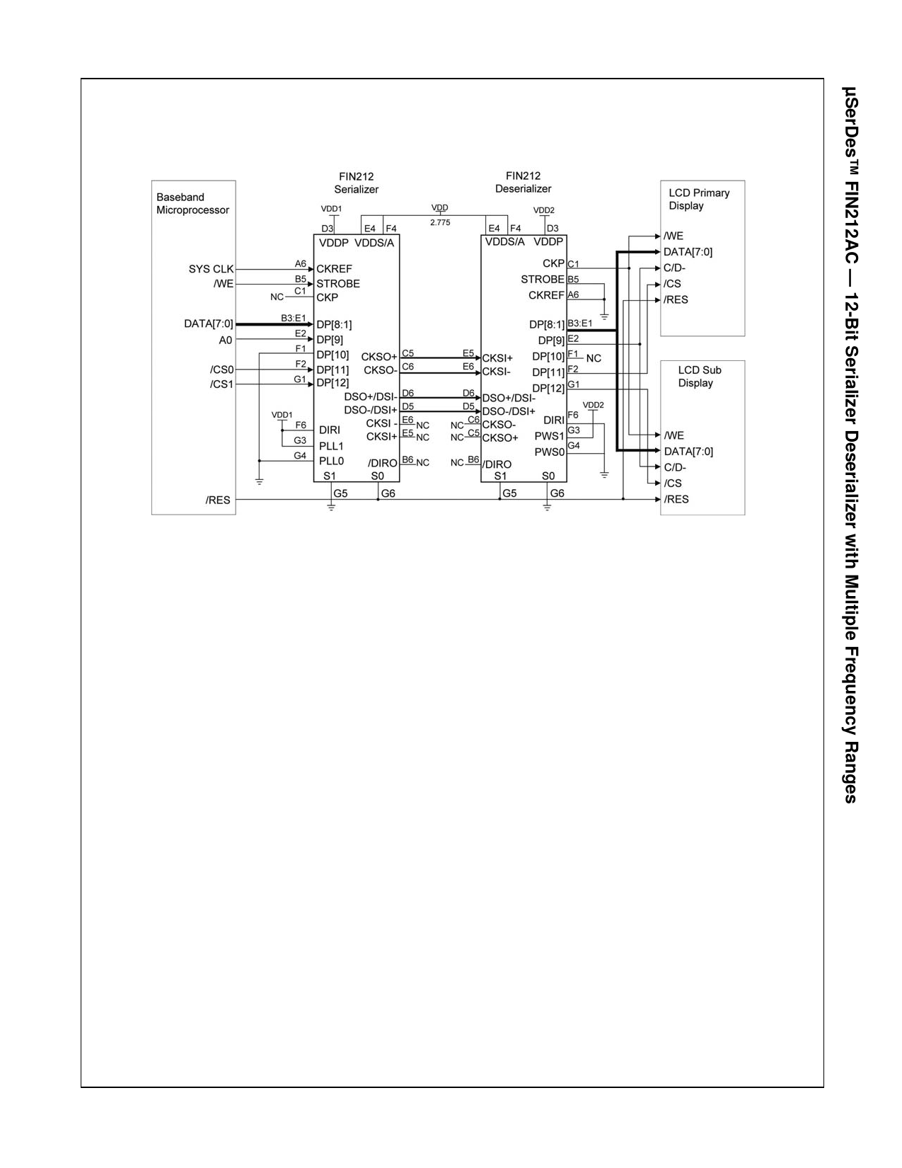
Figure 6. Dual Display with 8-Bit WRITE-Only Microcontroller Interface
(Example Shows BGA 42-Pin Package)
Serializer Configuration:
PLL Frequency Mode: MODE 1 (S1=0, S0=1) CKREF=26MHz
STROBE Frequency = 10 MHz
PLL Divide Mode: Divide-by 2 (PLL1=1, PLL0=0) Multiplier x 3.5
Deserializer Configuration:
Edge Rate Mode: SLOW MODE 1 (S1=1, S0=0)
Pulse Width Mode: 13-Bit Time Mode (PWS1=PWS0=0) (~71.4ns)
Additional Application Information
Flex Cabling: The serial I/O information is transmitted at a high serial rate. Care must be taken implementing this
serial I/O flex cable. The following best practices should be used when developing the flex cabling or Flex PCB.
Keep all four differential Serial Wires the same length.
Do not allow noisy signals over or near differential serial wires.
Example: No LVCMOS traces over differential serial wires.
Use only one ground plane or wire over the differential serial wires. Do not run ground over top and bottom.
Design goal of 100-ohms differential characteristic impedance.
Do not place test points on differential serial wires.
Use differential serial wires a minimum of 2cm away from the antenna.
For additional applications notes or flex guidelines see your sales rep or contact Fairchild directly.
© 2006 Fairchild Semiconductor Corporation
FIN212AC Rev. 1.0.6
10
www.fairchildsemi.com
Share Link: