FM24CL04 查看數據表(PDF) - Unspecified
零件编号
产品描述 (功能)
生产厂家
FM24CL04 Datasheet PDF : 12 Pages
| |||
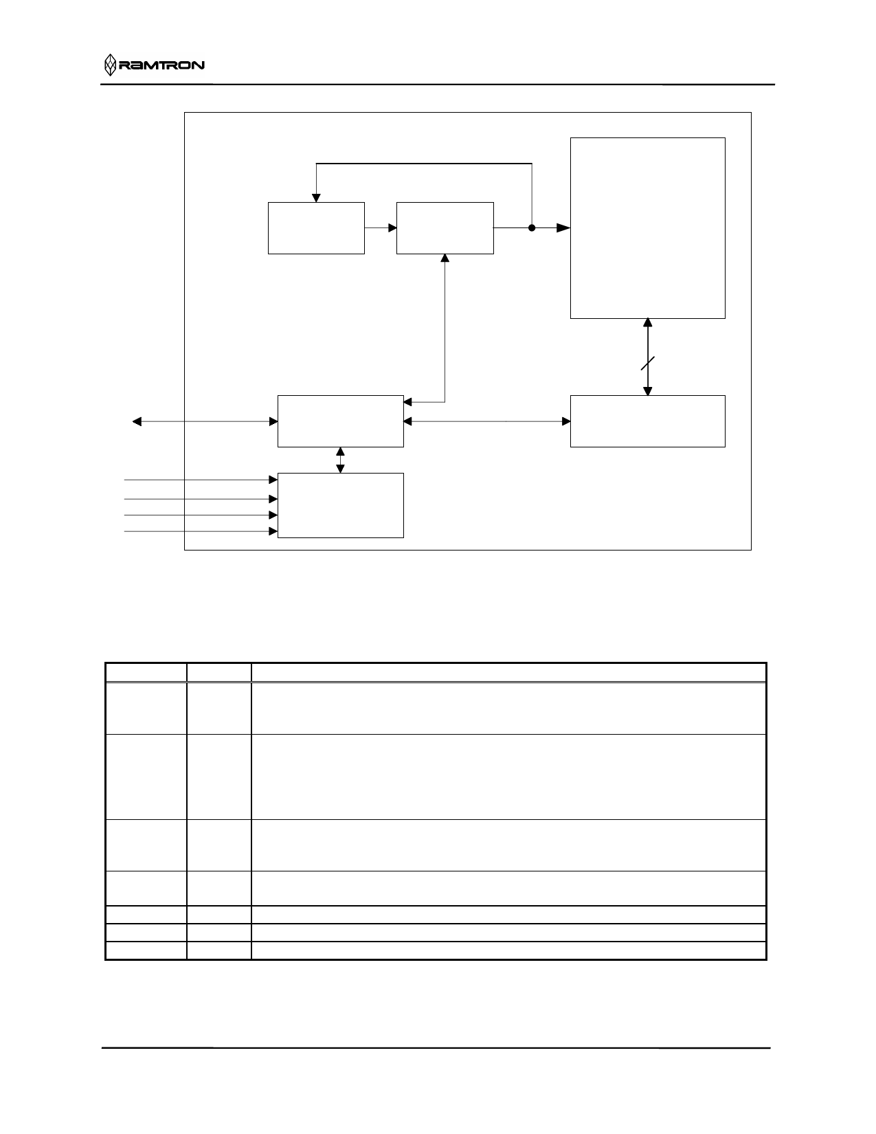
FM24CL04
Counter
Address
Latch
128 x 32
FRAM Array
`
SDA
SCL
WP
A1
A2
Serial to Parallel
Converter
Control Logic
Figure 1. Block Diagram
8
Data Latch
Pin Description
Pin Name
A1-A2
I/O
Input
SDA
I/O
SCL
WP
NC
VDD
VSS
Input
Input
-
Supply
Supply
Pin Description
Address 1-2: The address pins set the device select address. The device address value
in the 2-wire slave address must match the setting of these two pins. These pins are
internally pulled down.
Serial Data/Address: This is a bi-directional pin used to shift serial data and addresses
for the two-wire interface. It employs an open-drain output and is intended to be wire-
OR’d with other devices on the two-wire bus. The input buffer incorporates a Schmitt
trigger for noise immunity and the output driver includes slope control for falling
edges. A pull-up resistor is required.
Serial Clock: The serial clock input for the two-wire interface. Data is clocked out of
the device on the SCL falling edge, and clocked in on the SCL rising edge. The SCL
input also incorporates a Schmitt trigger input for improved noise immunity.
Write Protect: When WP is high the entire array is write protected. When WP is low,
all addresses may be written. This pin is internally pulled down.
No connect
Supply Voltage
Ground
Rev. 2.0
July 2003
Page 2 of 12
Share Link: 