FM24C64 查看數據表(PDF) - Ramtron International Corporation
零件编号
产品描述 (功能)
生产厂家
FM24C64 Datasheet PDF : 12 Pages
| |||
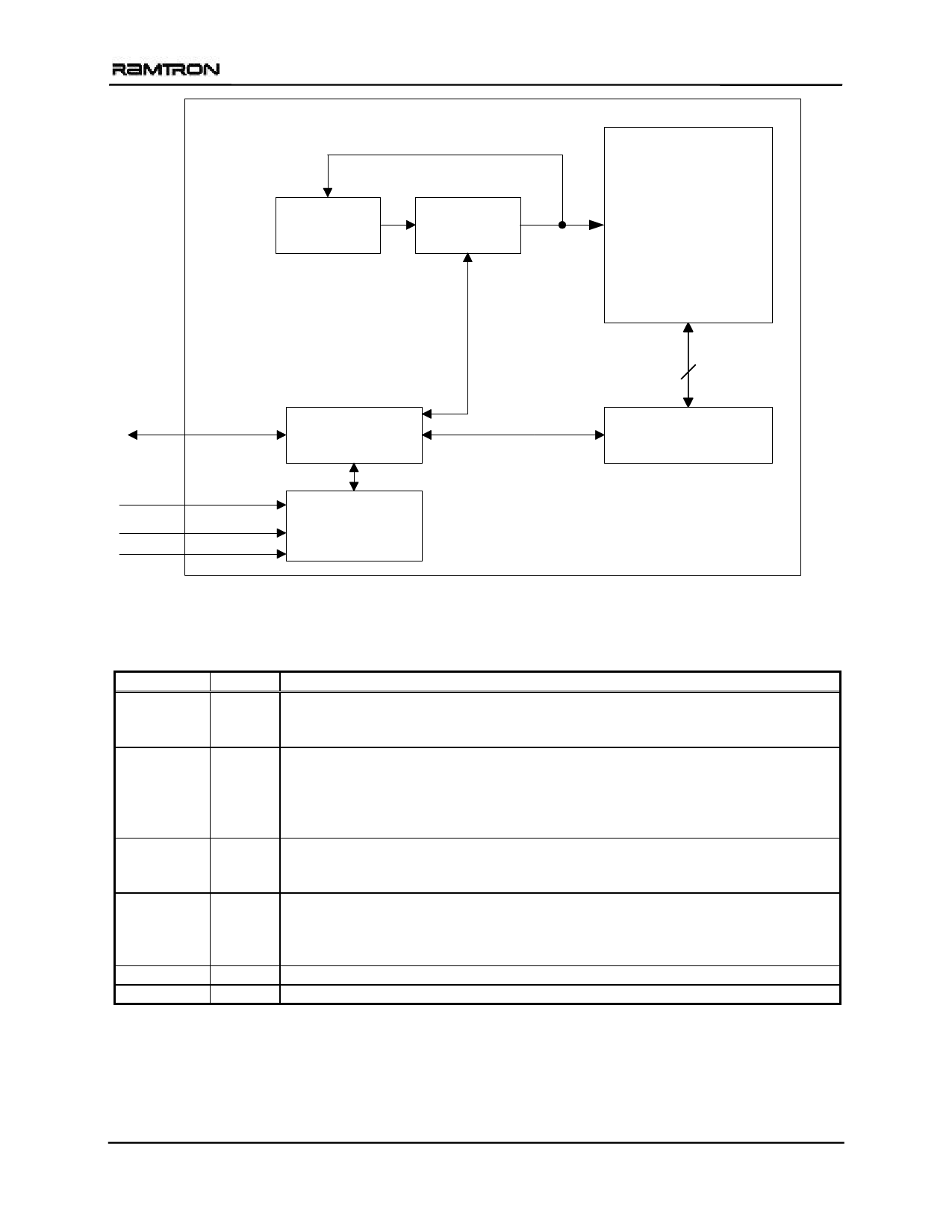
FM24C64
Counter
Address
Latch
1,024 x 64
FRAM Array
8
SDA
SCL
WP
A0-A2
Serial to Parallel
Converter
Control Logic
Data Latch
Figure 1. FM24C64 Block Diagram
Pin Description
Pin Name
A0-A2
I/O
Input
SDA
I/O
SCL
WP
VDD
VSS
Input
Input
Supply
Supply
Pin Description
Address 2-0: These pins are used to select one of up to 8 devices of the same type on
the same two-wire bus. To select the device, the address value on the three pins must
match the corresponding bits contained in the device address.
Serial Data Address: This is a bi-directional pin used to shift serial data and addresses
for the two-wire interface. It employs an open-drain output and is intended to be wire-
OR’d with other devices on the two-wire bus. The input buffer incorporates a Schmitt
trigger for noise immunity and the output driver includes slope control for falling
edges. A pull-up resistor is required.
Serial Clock: The serial clock input for the two-wire interface. Data is clocked out of
the device on the SCL falling edge, and clocked in on the SCL rising edge. The SCL
input also incorporates a Schmitt trigger input for improved noise immunity.
Write Protect: When WP is high, addresses in the upper quadrant of the logical
memory map will be write-protected. Write access is permitted to the lower three-
quarters of the address space. When WP is low, all addresses may be written. This pin
must not be left floating.
Supply Voltage: 5V
Ground
Rev. 3.0
Mar. 2005
2 of 12
Share Link: 