FM24C64 查看數據表(PDF) - Ramtron International Corporation
零件编号
产品描述 (功能)
生产厂家
FM24C64 Datasheet PDF : 12 Pages
| |||
Address and Data
By Master Start
DEVICE ADDRESS
ADDRESS MSB
S
0 A XXX
By FM24C64
ADDRESS LSB
A
A
ACKNOWLEDGE
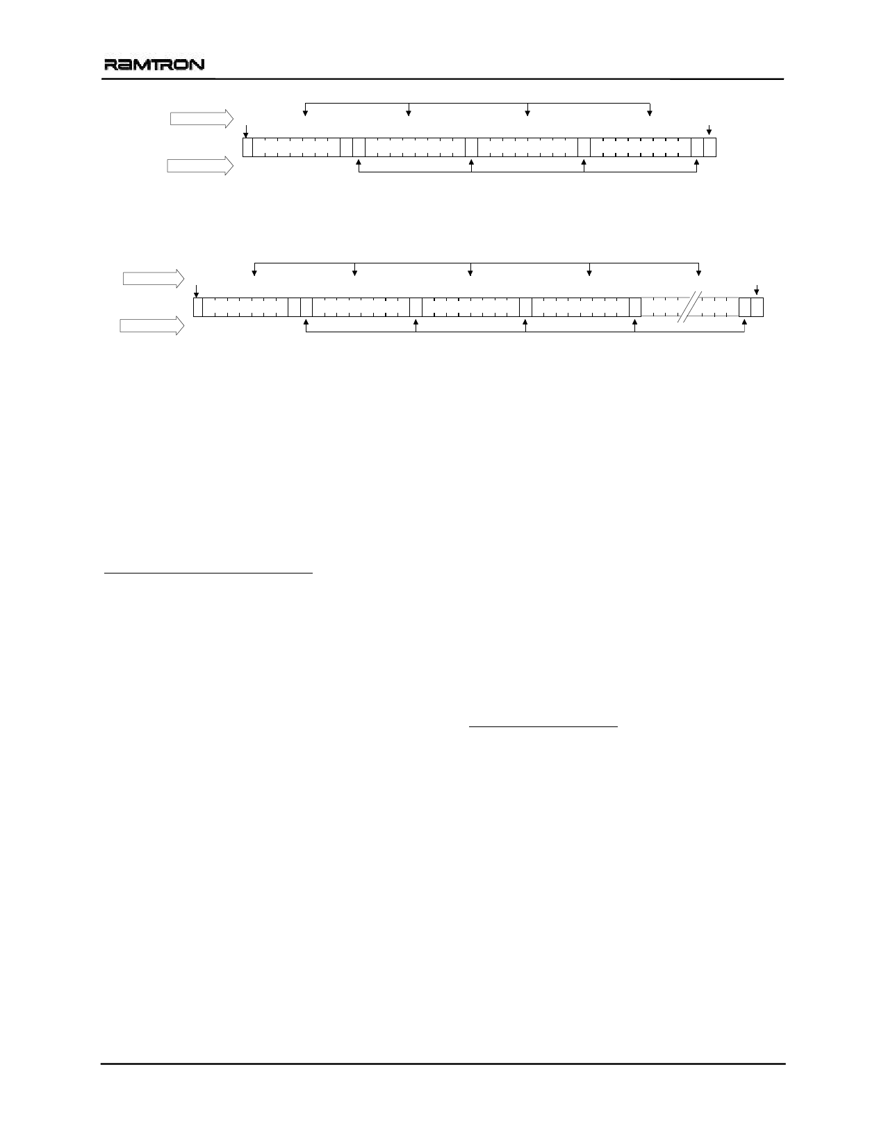
Figure 5. Byte Write
FM24C64
DATA BYTE
Stop
AP
Address and Data
By Master Start
DEVICE ADDRESS
ADDRESS MSB
S
0 A XXX
By FM24C64
ADDRESS LSB
A
A
ACKNOWLEDGE
Figure 6. Multiple Byte Write
DATA BYTE
A
DATA BYTE
Stop
AP
Read Operation
There are two basic types of read operations. They
are current address read and selective address read. In
a current address read, the FM24C64 uses the internal
address latch to supply the address. In a selective
read, the user performs a procedure to set the address
to a specific value.
Current Address & Sequential Read
The FM24C64 uses an internal latch to supply the
address for a read operation. A current address read
uses the existing value in the address latch as a
starting place for the read operation. The system
reads from the address immediately following that of
the last operation.
To perform a current address read, the bus master
supplies a device address with the LSB set to 1. This
indicates that a read operation is requested. After
receiving the complete device address, the FM24C64
will begin shifting out data from the current address
on the next clock. The current address is the value
held in the internal address latch. Beginning with the
current address, the bus master can read any number
of bytes. Thus, a sequential read is simply a current
address read with multiple byte transfers. After each
byte the internal address counter will be incremented.
Each time the bus master acknowledges a byte, this
indicates that the FM24C64 should read out the next
sequential byte.
There are four ways to properly terminate a read
operation. Failing to properly terminate the read will
likely create a bus contention as the FM24C64
attempts to read out additional data onto the bus. The
four valid methods are:
1. The bus master issues a no-acknowledge in the
9th clock cycle and a stop in the 10th clock cycle.
This is illustrated in Figures 7-9. This is the
preferred method.
2. The bus master issues a no-acknowledge in the
9th clock cycle and a start in the 10th.
3. The bus master issues a stop in the 9th clock
cycle.
4. The bus master issues a start in the 9th clock
cycle.
If the internal address reaches 1FFFh, it will wrap
around to 0000h on the next read cycle. Figures 7 and
8 show the proper operation for current address reads.
Selective (Random) Read
There is a simple technique that allows a user to
select a random address location as the starting point
for a read operation. This involves using the first
three bytes of a write operation to set the internal
address followed by subsequent read operations.
To perform a selective read, the bus master sends out
the device address with the LSB set to 0. This
specifies a write operation. According to the write
protocol, the bus master then sends the address bytes
that are loaded into the internal address latch. After
the FM24C64 acknowledges the address, the bus
master issues a start condition. This simultaneously
aborts the write operation and allows the read
command to be issued with the device address LSB
set to a 1. The operation is now a current address
read.
Rev. 3.0
Mar. 2005
6 of 12
Share Link: 