LCX028AMT 查看數據表(PDF) - Sony Semiconductor
零件编号
产品描述 (功能)
生产厂家
LCX028AMT Datasheet PDF : 25 Pages
| |||
LCX028AMT
Input Signals
1. Input signal voltage conditions (VSS = 0V)
Item
Symbol
Min.
H shift register input voltage (Low) VHIL
–0.5
HST, HCK1, HCK2, RGT (High) VHIH
4.5
Typ.
0.0
5.0
Max.
Unit
0.4
V
5.5
V
V shift register input voltage (Low) VVIL
–0.5
0.0
VB1, VB2, BLK, VST,
VCK, PCG, ENB, DWN (High) VVIH
4.5
5.0
0.4
V
5.5
V
Video signal center voltage
Video signal input range∗1
Common voltage of panel∗2
Uniformity improvement signal
input voltage (PSIG)∗3
VVC
6.9
7.0
7.1
V
Vsig
VVC – 4.5
7.0
VVC + 4.5 V
Vcom VVC – 0.6 VVC – 0.5 VVC – 0.4 V
VpsigB VVC ± 4.4 VVC ± 4.5 VVC ± 4.6
VpsigG VVC ± 1.7 VVC ± 1.8 VVC ± 1.9 V
∗1 Input video signal shall be symmetrical to VVC.
∗2 The typical value of the common pad voltage may lower its suitable voltage according to the set
construction to use. In this case, use the voltage of which has maximum contrast as typical value.
When the typical value is lowered, the maximum and minimum values may lower.
∗3 Input a uniformity improvement signal PSIG in the same polarity with video signals VSIG1 to VSIG12 and
which is symmetrical to VVC. PSIG wave form is 2 steps like below, in the upper chart, upper shows signal
level of the 1st step, lower shows signal level of the 2nd step. Also, the rising and falling of PSIG are
synchronized with the rising of PCG pulse, and the rise time trPSIG and fall time tfPSIG are suppressed
within 400ns (as shown in a diagram below).
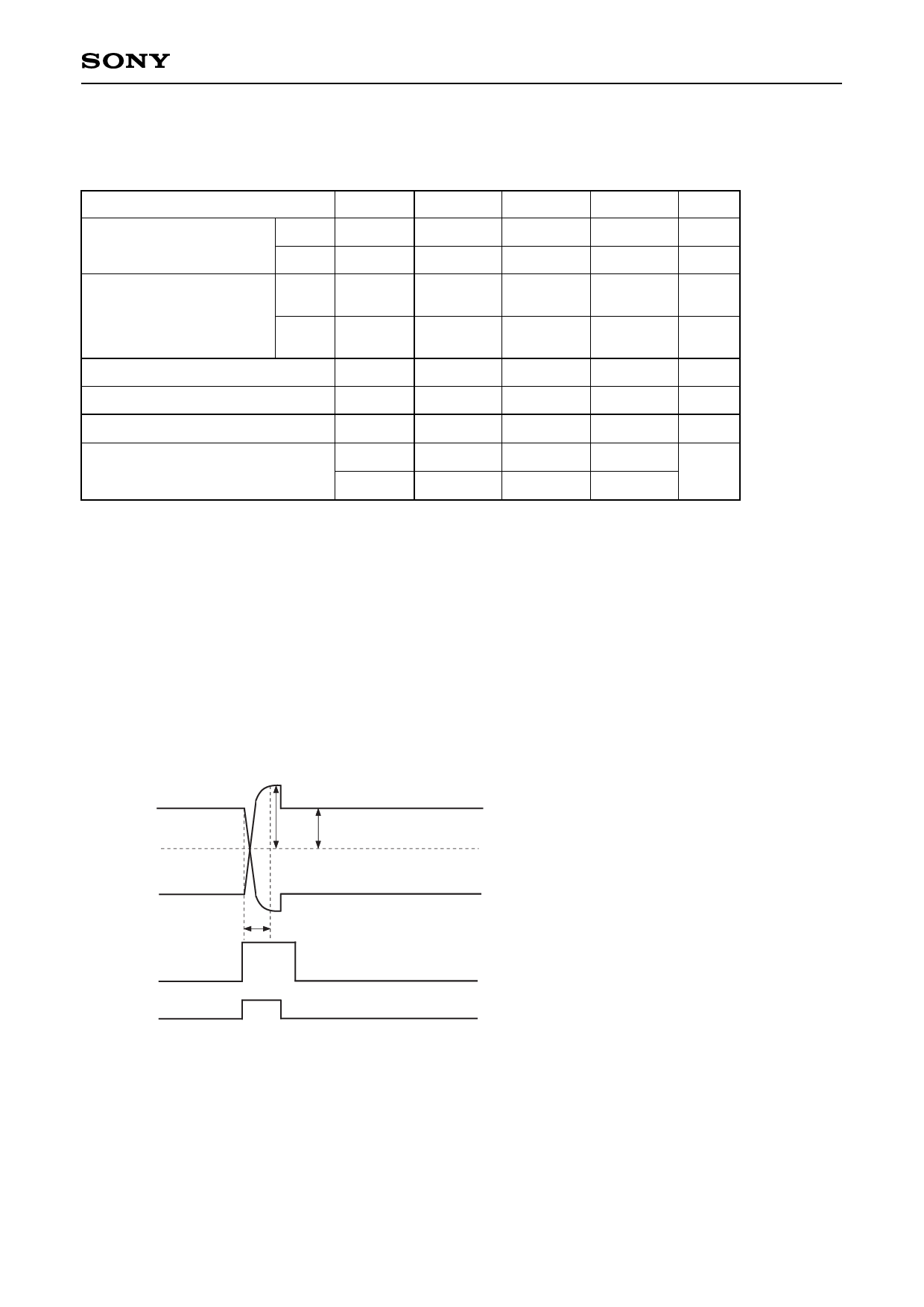
Input waveform of uniformity improvement signal PSIG
PSIG
90%
PsigB
PsigG
VVC
PCG
10%
trPSIG
tfPSIG
PRG∗4
∗4 PRG shows the time of the 1st step of PSIG signal, and it is not input to the panel.
Level Conversion Circuit
The LCX028AMT has a built-in level conversion circuit in the clock input unit on the panel. The input signal
level increases to HVDD or VVDD. The VCC of external ICs are applicable to 5 ± 0.5V.
–6–
Share Link: 