AZ100EL57DR2 查看數據表(PDF) - AZ Microtek
零件编号
产品描述 (功能)
生产厂家
AZ100EL57DR2 Datasheet PDF : 5 Pages
| |||
ARIZONA MICROTEK, INC.
AZ10EL57
AZ100EL57
ECL/PECL 4:1 Differential Multiplexer
FEATURES
• 75kΩ Internal Input Pulldown Resistors
• 2:1 Operation When SEL1 Not Connected
• Multiple VBB Outputs Allow Single-ended
Operation
• Direct Replacement for ON Semiconductor
MC10EL57 & MC100EL57
PACKAGE AVAILABILITY
PACKAGE
SOIC 16
SOIC 16 T&R
SOIC 16 T&R
SOIC 16
SOIC 16 T&R
SOIC 16 T&R
PART NO.
AZ10EL57D
AZ10EL57DR1
AZ10EL57DR2
AZ100EL57D
AZ100EL57DR1
AZ100EL57DR2
MARKING
AZM10EL57
AZM10EL57
AZM10EL57
AZM100EL57
AZM100EL57
AZM100EL57
DESCRIPTION
The AZ10/100EL57 is a fully differential 4:1 multiplexer. By leaving the SEL1 line open (pulled LOW via the
input pulldown resistor) the device can also be used as a differential 2:1 multiplexer with the SEL0 input selecting
between D0 and D1. The fully differential architecture of the EL57 makes it ideal for use in low skew applications
such as clock distribution.
SEL1 is the most significant select line. The binary number applied to the select inputs will select the same
numbered data input (i.e., 00 selects D0, 01 selects D1, etc.).
The EL57 provides two VBB outputs for single-ended use or a DC bias reference for AC coupling to the device.
For single-ended input applications, the VBB reference should be connected to one side of the Dn/D¯ n differential
input pair. The input signal is then fed to the other Dn/D¯ n input. The VBB pins should be used only as a bias for the
EL57 as its current sink/source capability is limited. When used, the VBB pins should be bypassed to ground via a
0.01µF capacitor.
NOTE: Specifications in the ECL/PECL tables are valid when thermal equilibrium is established.
FUNCTION TABLE
SEL1 SEL0
Q
L
L
D0
L
H
D1
H
L
D2
H
H
D3
PIN DESCRIPTION
PIN
D0, D¯¯0 – D3, D¯¯3
SEL0, SEL1
VBB1, VBB2
Q, Q¯
VCC
VEE
FUNCTION
Data Input Pairs
Mux Select Inputs
Reference Outputs
Data Outputs
Positive Supply
Negative Supply
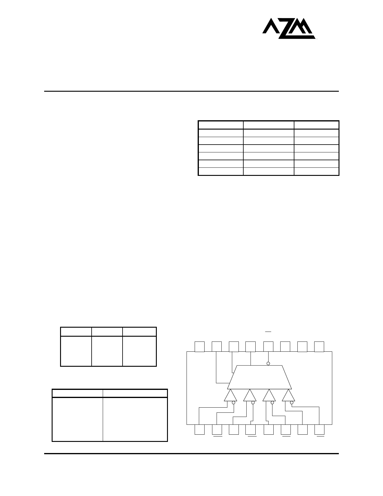
LOGIC DIAGRAM AND PINOUT ASSIGNMENT
V CC SEL0 SEL1 Q
16 15 14 13
Q VBB1 VBB2 VEE
12 11 10 9
4:1
1
2
3
4
5
6
7
8
D0 D0 D1 D1 D2 D2 D3 D3
1630 S. STAPLEY DR., SUITE 125 • MESA, ARIZONA 85204 • USA • (480) 962-5881 • FAX (480) 890-2541
www.azmicrotek.com
Share Link: 