GS8170DW72C-300I 查看數據表(PDF) - Giga Semiconductor
零件编号
产品描述 (功能)
生产厂家
GS8170DW72C-300I Datasheet PDF : 27 Pages
| |||
GS8170DW36/72C-333/300/250/200
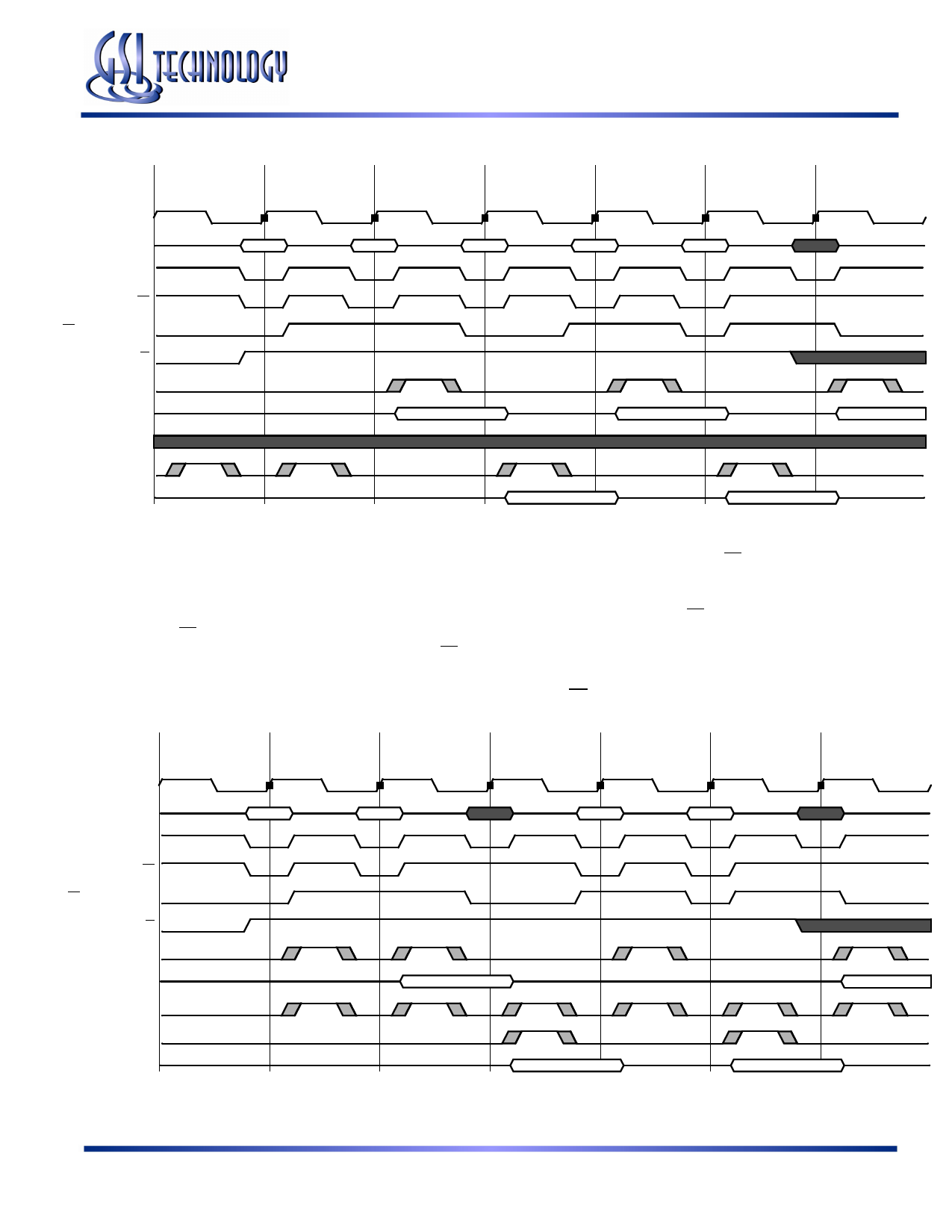
Echo Clock Control in Two Banks of SigmaRAMs
Read A
Read B
Read C
Read D
Read E
CK
Address
ADV
E1
E2 Bank1 E2 Bank1
W
CQ Bank1
DQ_Bank1
CQ1+CQ2
CQ Bank2
DQ_Bank2
A
B
C
D
E
Q(A)
Q(B)
Q(C)
Q(D)
Q(C)
It should be noted that deselection of the RAM via E2 and E3 also deselects the Echo Clock output drivers. The deselection of
Echo Clock drivers is always pipelined to the same degree as output data. Deselection of the RAM via E1 does not deactivate the
Echo Clocks.
In some applications it may be appropriate to pause between banks; to deselect both RAMs with E1 before resuming read
operations. An E1 deselect at a bank switch will allow at least one clock to be issued from the new bank before the first read cycle
in the bank. Although the following drawing illustrates a E1 read pause upon switching from Bank 1 to Bank 2, a write to Bank 2
would have the same effect, causing the RAM in Bank 2 to issue at least one clock before it is needed.
Pipelined Read Bank Switch with E1 Deselect
Read A
Read B
Deselect
Read D
Read E
CK
Address
ADV
E1
E2 Bank1 E2 Bank1
W
CQ_Bank1
DQ_Bank1
CQ1+CQ2
CQ_Bank2
DQ_Bank2
A
B
D
E
Q(A)
Q(B)
Q(E)
Q(D)
Rev: 2.04 5/2005
11/27
Specifications cited are subject to change without notice. For latest documentation see http://www.gsitechnology.com.
© 2002, GSI Technology, Inc.
Share Link: 