GS8170DW36C-333I 查看數據表(PDF) - Giga Semiconductor
零件编号
产品描述 (功能)
生产厂家
GS8170DW36C-333I Datasheet PDF : 27 Pages
| |||
GS8170DW36/72C-333/300/250/200
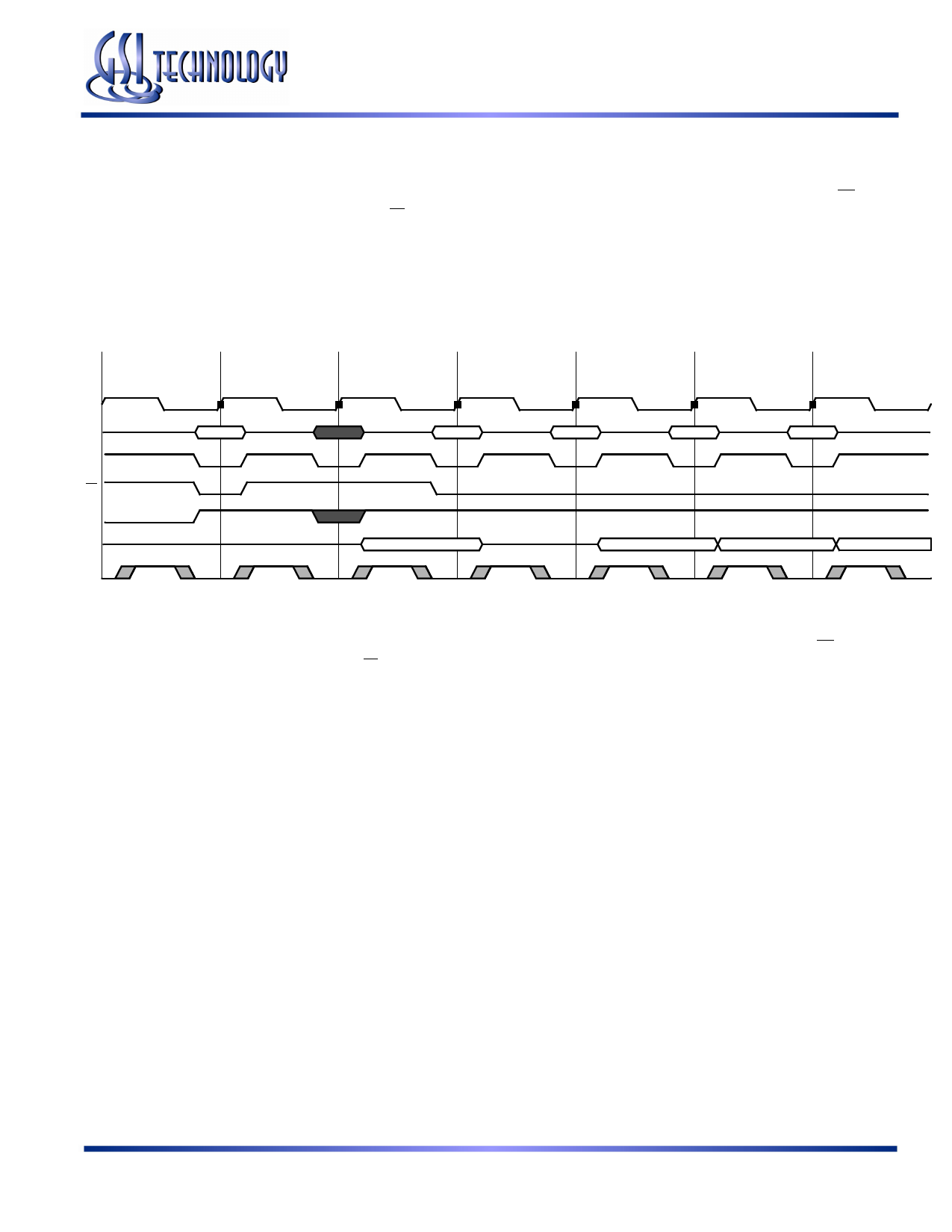
Read Operations
Pipelined Read
Read operation is initiated when the following conditions are satisfied at the rising edge of clock: All three chip enables (E1, E2,
and E3) are active, the write enable input signal (W) is deasserted high, and ADV is asserted low. The address presented to the
address inputs is latched into the address register and presented to the memory core and control logic. The control logic determines
that a read access is in progress and allows the requested data to propagate to the input of the output register. At the next rising edge
of clock the read data is allowed to propagate through the output register and onto the output pins
Single Data Rate (SDR) Pipelined Read.
Read A
Deselect
Read B
Read C
Read D
CK
Address
A
ADV
E1
W
DQ
CQ
B
Q(A)
C
D
E
Q(B)
Q(C)
Q(D)
Write Operations
Write operation occurs when the following conditions are satisfied at the rising edge of clock: All three chip enables (E1, E2, and
E3) are active, the write enable input signal (W) is asserted low, and ADV is asserted low.
Rev: 2.04 5/2005
5/27
Specifications cited are subject to change without notice. For latest documentation see http://www.gsitechnology.com.
© 2002, GSI Technology, Inc.
Share Link: 