HA-2510 查看數據表(PDF) - Intersil
零件编号
产品描述 (功能)
生产厂家
HA-2510 Datasheet PDF : 7 Pages
| |||
HA-2510/883
Absolute Maximum Ratings
Thermal Information
Voltage Between V+ and V- Terminals . . . . . . . . . . . . . . . . . . . .40V
Differential Input Voltage . . . . . . . . . . . . . . . . . . . . . . . . . . . . . . .15V
Voltage at Either Input Terminal . . . . . . . . . . . . . . . . . . . . . V+ to V-
Peak Output Current . . . . . . . . . . . . . . . . . . . . . . . . . . . . . . . . 50mA
ESD Rating . . . . . . . . . . . . . . . . . . . . . . . . . . . . . . . . . . . . . .<2000V
Operating Conditions
Temperature Range. . . . . . . . . . . . . . . . . . . . . . . . . -55oC to 125oC
Supply Voltage . . . . . . . . . . . . . . . . . . . . . . . . . . . . . . . . . . . . . . . . . ±15V
VINCM ≤ 1/2 (V+ - V-)
RL ≥ 2kΩ
Thermal Resistance (Typical, Note 1)
θJA
θJC
Metal Can Package . . . . . . . . . . . . . . . . . 160oC/W 75oC/W
CERDIP Package. . . . . . . . . . . . . . . . . . . 120oC/W 30oC/W
Package Power Dissipation Limit at 75oC for TJ ≤ 175oC
Metal Can Package . . . . . . . . . . . . . . . . . . . . . . . . . . . . . .625mW
CERDIP Package. . . . . . . . . . . . . . . . . . . . . . . . . . . . . . . .870mW
Package Power Dissipation Derating Factor Above 75oC
Metal Can Package . . . . . . . . . . . . . . . . . . . . . . . . . . . 6.3mW/oC
CERDIP Package. . . . . . . . . . . . . . . . . . . . . . . . . . . . . 8.7mW/oC
Maximum Junction Temperature . . . . . . . . . . . . . . . . . . . . . . .175oC
Maximum Storage Temperature Range . . . . . . . . . -65oC to 150oC
Maximum Lead Temperature (Soldering 10s) . . . . . . . . . . . . .300oC
CAUTION: Stresses above those listed in “Absolute Maximum Ratings” may cause permanent damage to the device. This is a stress only rating and operation of the
device at these or any other conditions above those indicated in the operational sections of this specification is not implied.
NOTE:
1. θJA is measured with the component mounted on a low effective thermal conductivity test board in free air. See Tech Brief TB379
for details.
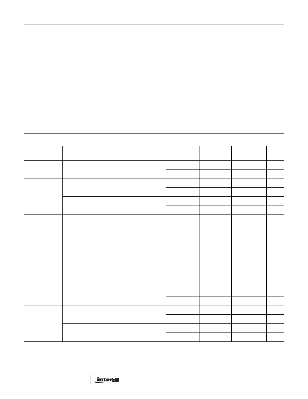
TABLE 1. DC ELECTRICAL PERFORMANCE CHARACTERISTICS
Device Tested at: VSUPPLY = ±15V, RSOURCE = 100Ω, RLOAD = 500kΩ, VOUT = 0V, Unless Otherwise Specified.
PARAMETER
SYMBOL
CONDITIONS
GROUP A
SUBGROUPS TEMP (oC)
MIN
MAX UNITS
Input Offset
Voltage
VIO
VCM = 0V
1
25
-8
8
mV
2, 3
125, -55
-18
10
mV
Input Bias Current
+IB
VCM = 0V, +RS = 100kΩ, -RS = 100Ω
1
25
-200 200
nA
2, 3
125, -55
-400 400
nA
-IB
VCM = 0V, +RS = 100Ω, -RS = 100kΩ
1
25
-200 200
nA
2, 3
125, -55
-400 400
nA
Input Offset
Current
IIO
VCM = 0V, +RS = 100kΩ, -RS = 100kΩ
1
25
-25
25
nA
2, 3
125, -55
-50
50
nA
Common Mode
Range
+CMR V+ = 5V, V- = -25V
1
25
+10
-
V
2, 3
125, -55
+10
-
V
-CMR V+ = 25V, V- = -5V
1
25
-
-10
V
2, 3
125, -55
-
-10
V
Large Signal
Voltage Gain
+AVOL VOUT = 0V and +10V, RL = 2kΩ
4
25
10
-
kV/V
5, 6
125, -55
7.5
-
kV/V
-AVOL VOUT = 0V and -10V, RL = 2kΩ
4
25
10
-
kV/V
5, 6
125, -55
7.5
-
kV/V
Common Mode
+CMRR ∆VCM = +10V, V+ = +5V, V- = -25V, VOUT
1
Rejection Ratio
= -10V
2, 3
25
80
-
dB
125, -55
80
-
dB
-CMRR ∆VCM = -10V, V+ = +25V, V- = -5V, VOUT =
1
+10V
2, 3
25
80
-
dB
125, -55
80
-
dB
2
FN3697.4
January 3, 2006
Share Link: 