HCPL-0730R2 查看數據表(PDF) - Fairchild Semiconductor
零件编号
产品描述 (功能)
生产厂家
HCPL-0730R2 Datasheet PDF : 12 Pages
| |||
SINGLE CHANNEL:
DUAL CHANNEL:
LOW INPUT CURRENT
HIGH GAIN SPLIT
DARLINGTON OPTOCOUPLERS
HCPL-0700
HCPL-0730
HCPL-0701
HCPL-0731
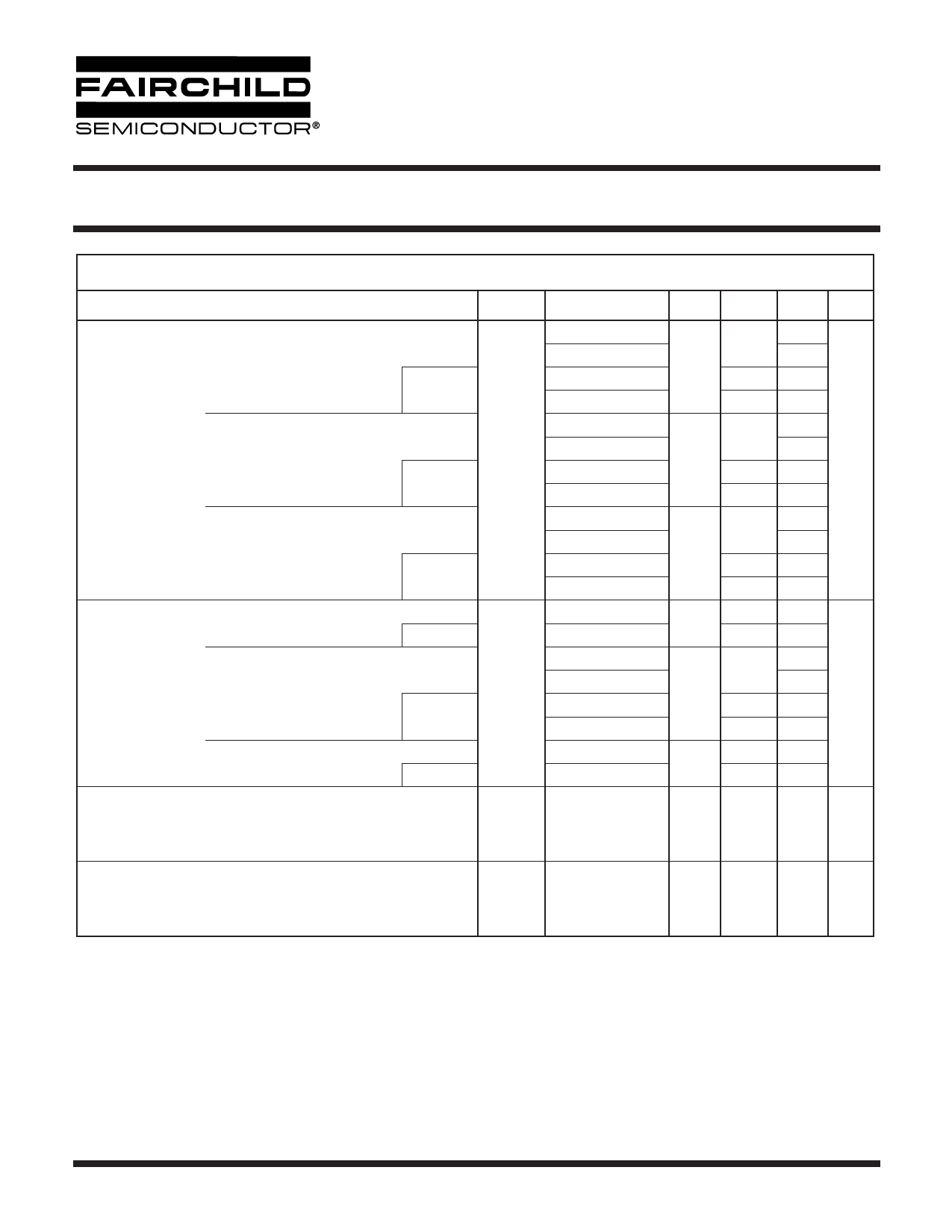
SWITCHING CHARACTERISTICS (TA = 0 to 70°C unless otherwise specified., VCC = 5 V)
Parameter
Test Conditions
Symbol
Device
Min Typ**
(RL = 4.7 kΩ, IF = 0.5 mA)
Propagation delay
time to logic low
(Note 2) (Fig. 14)
TA = 25°C
(RL = 270 Ω, IF = 12 mA)
TA = 25°C
(RL = 2.2 kΩ, IF = 1.6 mA)
TA = 25°C
Propagation delay
time to logic high
(Note 2) (Fig. 14)
(RL = 4.7 kΩ, IF = 0.5 mA)
TA = 25°C
(RL = 270 Ω, IF = 12 mA)
TA = 25°C
Common mode
transient
immunity at
logic high
(RL = 2.2 kΩ, IF = 1.6 mA)
TA = 25°C
(IF = 0 mA, |VCM| = 10 VP-P)
TA = 25°C (RL = 2.2 kΩ) (Note 3) (Fig. 15)
TPHL
TPLH
|CMH|
HCPL-0701
HCPL-0731
HCPL-0701
3
HCPL-0731
5
HCPL-0701
HCPL-0731
HCPL-0701
0.3
HCPL-0731
0.4
HCPL-0700
HCPL-0730/0731
HCPL-0700
1
HCPL-0730/0731
2
HCPL-0701/31
HCPL-0701/31
12
HCPL-0701
HCPL-0731
HCPL-0701
1.6
HCPL-0731
1.6
HCPL-0700/30/31
HCPL-0700/30/31
7
ALL
1,000 10,000
Common mode
transient
immunity at
logic low
(IF = 1.6 mA, |VCM| = 10 VP-P,
RL = 2.2 kΩ)
TA = 25°C (Note 3) (Fig. 15)
|CML|
ALL
1,000 10,000
Max
30
120
25
100
2
3
1
2
15
25
10
20
90
60
10
15
7
10
50
35
Unit
µs
µs
V/µs
V/µs
NOTES
1. Current Transfer Ratio is defined as a ratio of output collector current, IO, to the forward LED input current, IF, times 100%.
2. Pin 7 open. Use of a resistor between pins 5 and 7 will decrease gain and delay time.
3. Common mode transient immunity in logic high level is the maximum tolerable (positive) dVCM/dt on the leading edge of the
common mode pulse signal, VCM, to assure that the output will remain in a logic high state (i.e., VO>2.0 V). Common mode
transient immunity in logic low level is the maximum tolerable (negative) dVCM/dt on the trailing edge of the common mode
pulse signal, VCM, to assure that the output will remain in a logic low state (i.e., VO<0.8 V).
4. Device is considered a two terminal device: Pins 1, 2, 3 and 4 are shorted together and Pins 5, 6, 7 and 8 are shorted together.
5. 2500 VAC RMS for 1 minute duration is equivalent to 3000 VAC RMS for 1 second duration.
** All typicals at TA = 25°C
© 2005 Fairchild Semiconductor Corporation
Page 4 of 12
6/15/05
Share Link: 