HCPL-2200-500E 查看數據表(PDF) - Avago Technologies
零件编号
产品描述 (功能)
生产厂家
HCPL-2200-500E Datasheet PDF : 13 Pages
| |||
Notes:
1. Derate total package power dissipation, PT,
linearly above 70°C free air temperature at a
rate of 4.5 mW/°C.
2. Duration of output short circuit time should
not exceed 10 ms.
3. Device considered a two-terminal device:
pins 1, 2, 3, and 4 shorted together and pins
5, 6, 7, and 8 shorted together.
4. The tPLH propagation delay is measured
from the 50% point on the leading edge of
the input pulse to the 1.3 V point on the
leading edge of the output pulse. The tPHL
propagation delay is measured from the
50% point on the trailing edge of the input
pulse to the 1.3 V point on the trailing edge
of the output pulse.
5. When the peaking capacitor is omitted,
propagation delay times may increase by
100 ns.
6. CML is the maximum rate of rise of the
common mode voltage that can be
sustained with the output voltage in the
logic low state (VO < 0.8 V). CMH is the
maximum rate of fall of the common mode
voltage that can be sustained with the
output voltage in the logic high state
(VO > 2.0 V).
7. Use of a 0.1 µF bypass capacitor connected
between pins 5 and 8 is recommended.
8. In accordance with UL1577, each
optocoupler is proof tested by applying an
insulation test voltage ≥4500 V rms for one
second (leakage detection current limit, II-O
≤5 µA). This test is performed before the
100% production test for partial discharge
(Method b) shown in the IEC/EN/DIN EN
60747-5-2 Insulation Characteristics Table, if
applicable.
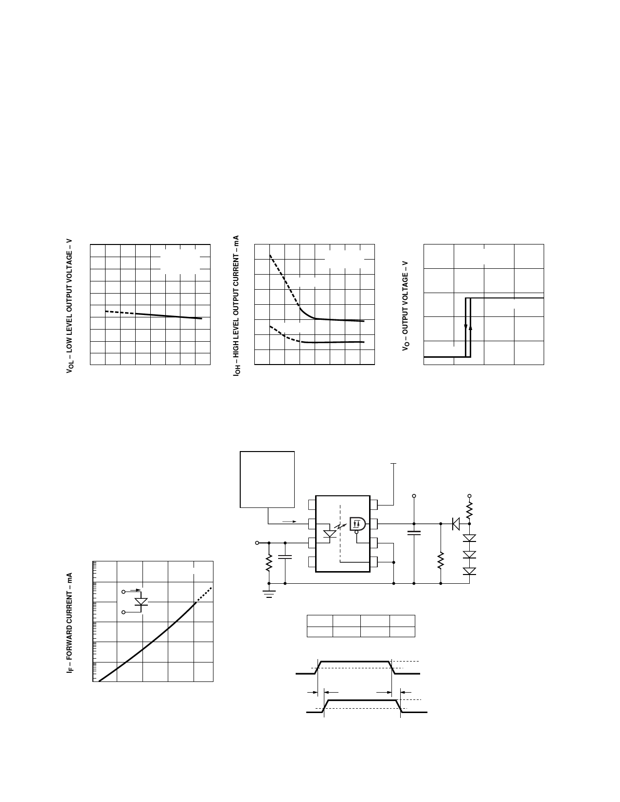
1.0
0.9
VCC = 4.5 V
IF = 0 mA
0.8
VO = 6.4 mA
0.7
0.6
0.5
0.4
0.3
0.2
0.1
0
-60 -40 -20 0
20 40 60 80 100
TA – TEMPERATURE – °C
0
-1
VCC = 4.5 V
IF = 5 mA
-2
VO = 2.7 V
-3
-4
-5
VO = 2.4 V
-6
-7
-8
-60 -40 -20 0 20 40 60 80 100
TA – TEMPERATURE – °C
5
VCC = 4.5 V
TA = 25 °C
4
3
IOH = -2.6 mA
2
1
IOL = 6.4 mA
0
0
0.5
1.0
1.5
2.0
IF – INPUT CURRENT – mA
Figure 1. Typical logic low output voltage vs.
temperature.
Figure 2. Typical logic high output current vs.
temperature.
Figure 3. Output voltage vs. forward input
current.
1000
100
10
1.0
IF
+
VF
–
TA = 25 °C
0.1
0.01
0.001
1.1 1.2 1.3 1.4 1.5
VF – FORWARD VOLTAGE – V
Figure 4. Typical input diode forward
characteristic.
10
PULSE GEN.
tr = tf = 5 ns
f = 100 kHz
10 % DUTY
CYCLE
VO = 5 V
1
INPUT
IF
2
MONITORING
NODE
3
R1
C1 = 4
120 pF
HCPL-2200
VCC 8
7
6
GND 5
VCC
OUTPUT VO
MONITORING
NODE
5V
D1
619 Ω
C2 =
D2
15 pF
D3
5 kΩ
D4
INPUT IF
THE PROBE AND JIG CAPACITANCES
ARE INCLUDED IN C1 AND C2.
RI 2.15 kΩ 1.10 kΩ 681 Ω
IF (ON) 1.6 mA 3 mA 5 mA
ALL DIODES ARE 1N916 OR 1N3064.
IF (ON)
50 % IF (ON)
0 mA
OUTPUT
VO
tPLH tPHL
VOH
1.3 V
VOL
Figure 5. Test circuit for tPLH, tPHL, tr, and tf.
Share Link: 