HD74LVC1G57CPE 查看數據表(PDF) - Renesas Electronics
零件编号
产品描述 (功能)
生产厂家
HD74LVC1G57CPE Datasheet PDF : 10 Pages
| |||
HD74LVC1G57
Configurable Multiple–Function Gate
Description
REJ03D0011–0300Z
Rev.3.00
Jun. 29, 2004
The HD74LVC1G57 has configurable multiple–function gate in a 6-pin package. The Output state is determined by
eight patterns of 3–bit input. The user can choose the logic functions AND, NAND, NOR, EX–NOR. Low voltage and
high-speed operation is suitable for the battery powered products (e.g., notebook computers), and the low power
consumption extends the battery life.
Features
• The basic gate function is lined up as renesas uni logic series.
• Supply voltage range: 1.65 to 5.5 V
Operating temperature range: –40 to +85°C
• All inputs VIH (Max.) = 5.5 V (@VCC = 0 V to 5.5 V)
All outputs VO (Max.) = 5.5 V (@VCC = 0 V)
• Output current:
±4 mA (@VCC = 1.65 V)
±8 mA (@VCC = 2.3 V)
±24 mA (@VCC = 3.0 V)
±32 mA (@VCC = 4.5 V)
• All the logical input has hysteresis voltage for the slow transition.
• Ordering Information
Part Name
Package Type
Package Code
Package
Abbreviation
HD74LVC1G57CPE WCSP-6 pin
TBS-6V
CP
HD74LVC1G57CLE
TBS-6AV
CL
Taping Abbreviation
(Quantity)
E (3,000 pcs/reel)
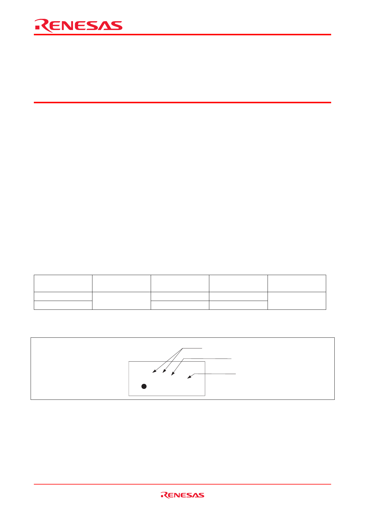
Article Indication
Marking
Year code
KRYM
Month code
Rev.3.00 Jun. 29, 2004 page 1 of 1
Share Link: 