HDD128M72D18RPW 查看數據表(PDF) - Hanbit Electronics Co.,Ltd
零件编号
产品描述 (功能)
生产厂家
HDD128M72D18RPW
Hanbit Electronics Co.,Ltd

HDD128M72D18RPW Datasheet PDF : 14 Pages
| |||
HANBit
HDD128M72D18RPW
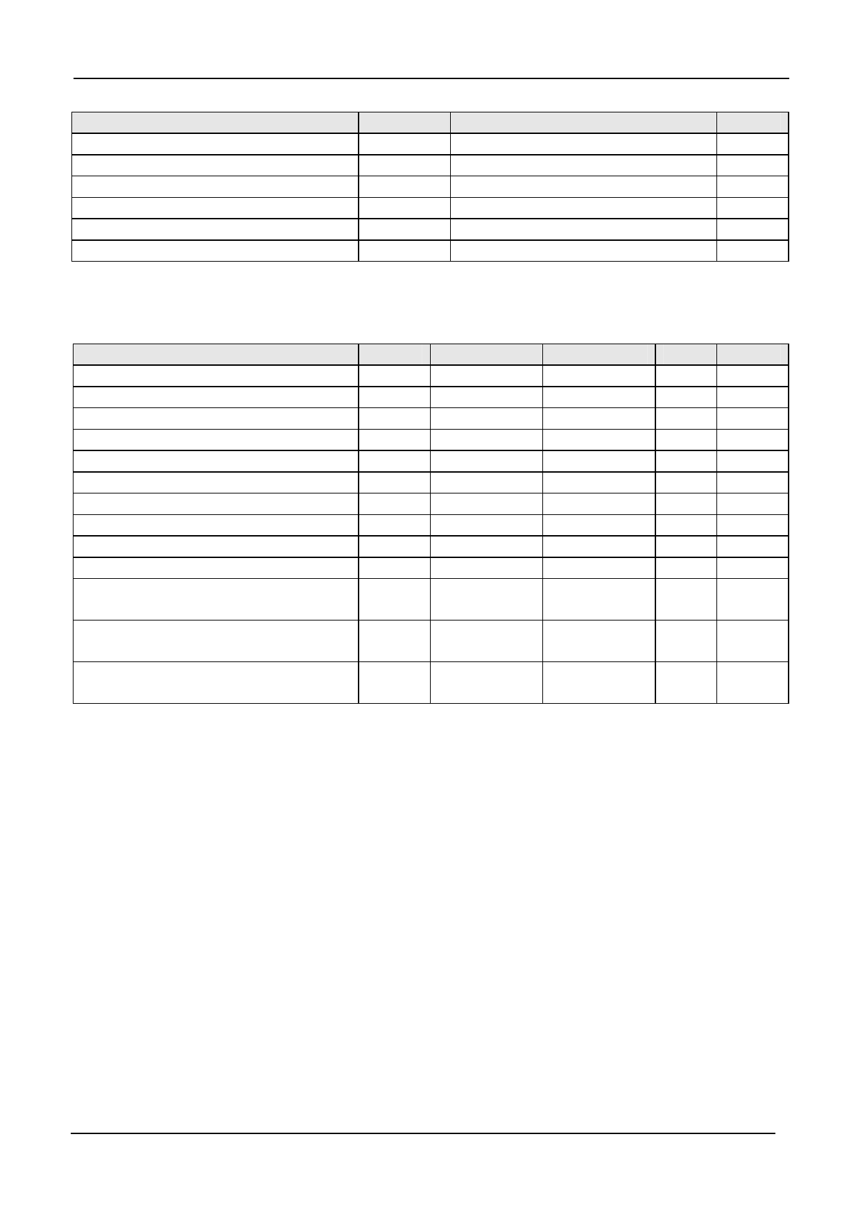
Absolute Maximum Ratings
PARAMETER
SYMBOL
RATING
Voltage on any pin relative to Vss
VIN, VOUT
-0.5 ~ 3.6
Voltage on VDD supply relative to Vss
VDD
-1.0 ~ 3.6
Voltage on VDDQ supply relative to Vss
VDDQ
-0.5 ~ 3.6
Storage temperature
TSTG
-55 ~ +150
Power dissipation
PD
1.5 * # of component
Short circuit current
IOS
50
Notes: Operation at above absolute maximum rating can adversely affect device reliability
UNTE
V
V
V
°C
W
mA
DC operating conditions
(Recommended operating conditions (Voltage referenced to Vss = 0V, TA = 0 to 70°C) )
PARAMETER
SYMBOL
MIN
Supply Voltage
VDD
2.3
I/O Supply Voltage
VDDQ
2.3
I/O Reference Voltage
I/O Termination Voltage(system)
VREF
VTT
0.49*VDDQ
VREF – 0.04
Input High Voltage
VIH (DC)
VREF + 0.15
Input Low Voltage
VIL (DC)
-0.3
Input Voltage Level, CK and /CK inputs
VIN (DC)
-0.3
Input Differential Voltage, CK and /CK inputs
VID (DC)
0.3
Input leakage current
I LI
-2
Output leakage current
I OZ
-5
Output High current (Normal strength driver)
; VOUT=VTT + 0.84V
I OH
-16.8
Output Low current (Normal strength driver)
; VOUT=VTT - 0.84V
I OL
16.8
Output High current (Half strength driver)
; VOUT=VTT + 0.45V
I OH
-9
MAX
2.7
2.7
0.51*VDDQ
VREF + 0.04
VREF + 0.3
VREF - 0.15
VDDQ + 0.3
VDDQ + 0.6
2
5
UNIT
V
V
V
V
V
V
V
V
uA
uA
mA
mA
mA
NOTE
1
2
3
Notes :
1. Includes ± 25mV margin for DC offset on VREF, and a combined total of ± 50mV margin for all AC noise and DC offset on VREF, bandwidth
limited to 20MHz. The DRAM must accommodate DRAM current spikes on VREF and internal DRAM noise coupled to VREF, both of which
may result in VREF noise. VREF should be de-coupled with an inductance of ≤ 3nH.
2.VTT is not applied directly to the device. VTT is a system supply for signal termination resistors, is expected to be set equal to VREF, and
must track variations in the DC level of VREF
3. VID is the magnitude of the difference between the input level on CK and the input level on /CK.
4. These parameters should be tested at the pin on actual components and may be checked at either the pin or the pad in simulation. The
AC and DC input specifications are relative to a VREF envelop that has been bandwidth limited to 200MHZ.
URL : www.hbe.co.kr
REV 1.0 (January. 2005)
5
HANBit Electronics Co.,Ltd.
Share Link: