HI-6011CDT 查看數據表(PDF) - Holt Integrated Circuits
零件编号
产品描述 (功能)
生产厂家
HI-6011CDT Datasheet PDF : 13 Pages
| |||
HI-6011
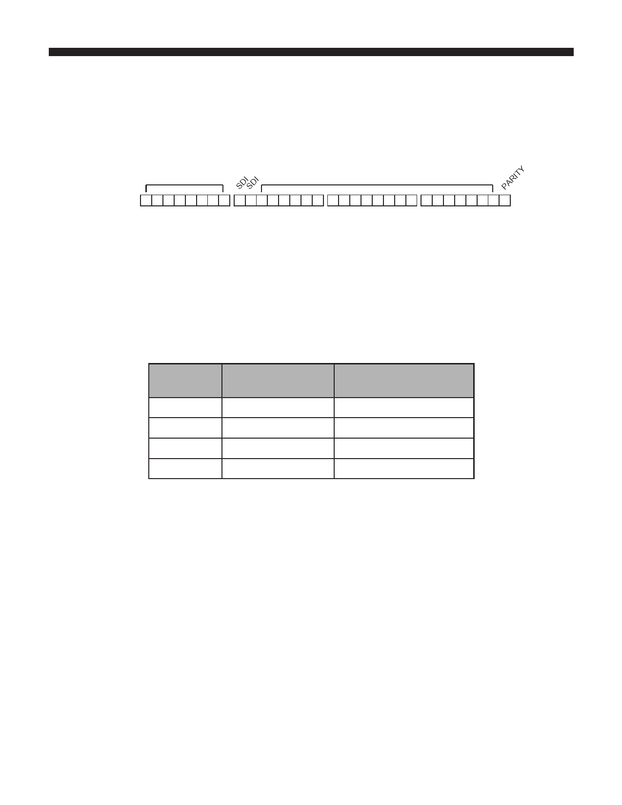
ARINC 429 DATA FORMAT AND READ/WRITE CYCLES
The ARINC 429 specification defines the 32-bit word as shown in Figure 1, indicating the order in which bits appear
on the ARINC 429 data bus. ARINC bit 1 is defined as the label MSB, whereas the data field MSB is bit 31 as shown
below.
MSB LABEL LSB
ARINC bit #: 1 2 3 4 5 6 7 8
SDISDI LSB
DATA
MSB
9 10 11 12 13 14 15 16 17 18 19 20 21 22 23 24 25 26 27 28 29 30 31 32
Figure 1. ARINC 429 Data Format.
Read/write operations to the HI-6011 are performed via 3 address pins, A2:0, and 8 data pins, D7:0. The address
pins A2:0 specify the possible read/write operations (see Section “Read/Write Operations”). The 32-bit ARINC word is
communicated using 4 successive reads or writes over the 8-bit data bus as follows:
Table 2. Order of ARINC 429 word bits during read/write cycles.
Read/Write
Cycle
ARINC 429 bits
1
Bits 1-8 (Label)
2
Bits 9-16
3
Bits 17-24
4
Bits 25-32
Data Pins D7:0
Bit 1 = D0, Bit 8 = D7
Bit 9 = D0, Bit 16 = D7
Bit 17 = D0, Bit 24 = D7
Bit 25 = D0, Bit 32 = D7
HOLT INTEGRATED CIRCUITS
4
Share Link: 