5962-88690013A 查看數據表(PDF) - Intersil
零件编号
产品描述 (功能)
生产厂家
5962-88690013A Datasheet PDF : 8 Pages
| |||
HM-6642
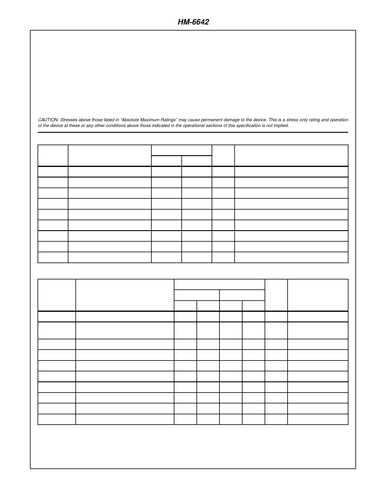
Absolute Maximum Ratings
Thermal Information
Supply Voltage . . . . . . . . . . . . . . . . . . . . . . . . . . . . . . . . . . . . . +7.0V
Input, Output or I/O Voltage . . . . . . . . . . . GND -0.3V to VCC +0.3V
Typical Derating Factor . . . . . . . . . . . . 5mA/MHz Increase in ICCOP
ESD Classification . . . . . . . . . . . . . . . . . . . . . . . . . . . . . . . . Class 1
Operating Conditions
Operating Voltage Range . . . . . . . . . . . . . . . . . . . . . +4.5V to +5.5V
Operating Temperature Range
HM-6642B-9, HM-6642-9 . . . . . . . . . . . . . . . . . . . -40oC to +85oC
Thermal Resistance
SBDIP Package . . . . . . . . . . . . . . . . . .
52θoJCA/W
14θoJCC/W
Slim SBDIP . . . . . . . . . . . . . . . . . . . . . 70oC/W
19oC/W
CLCC Package . . . . . . . . . . . . . . . . . . 58oC/W
14oC/W
Maximum Storage Temperature Range . . . . . . . . .-65oC to +150oC
Maximum Junction Temperature . . . . . . . . . . . . . . . . . . . . . . +175oC
Maximum Lead Temperature (Soldering 10s)+300oC
Die Characteristics
Gate Count . . . . . . . . . . . . . . . . . . . . . . . . . . . . . . . . . . . 1680 Gates
CAUTION: Stresses above those listed in “Absolute Maximum Ratings” may cause permanent damage to the device. This is a stress only rating and operation
of the device at these or any other conditions above those indicated in the operational sections of this specification is not implied.
DC Electrical Specifications
VCC = 5V ± 10%; TA = -40oC to +85oC (HM-6642B-9, HM-6642-9)
LIMITS
SYMBOL
PARAMETER
MIN
MAX UNITS
TEST CONDITIONS
ICCSB Standby Supply Current
-
100
µA IO = 0, VI = VCC or GND, VCC = 5.5V
ICCOP Operating Supply Current (Note 3)
-
20
mA f = 1MHz, IO = 0, VI = VCC or GND, VCC = 5.5V
II
Input Leakage Current
IOZ
Output Leakage Current
-1.0
+1.0
µA GND ≤ VI ≤ VCC, VCC = 5.5V
-1.0
+1.0
µA GND ≤ VO ≤ VCC, VCC = 5.5V
VIL
Input Low Voltage
-0.3
0.8
V VCC = 4.5V
VIH
Input High Voltage
2.4
VCC + 0.3
V
VCC = 5.5V
VOL Output Low Voltage
-
0.4
V IOL = 3.2mA, VCC = 4.5V
VOH1 Output High Voltage
2.4
-
V IOH = -1.0mA, VCC = 4.5V
VOH2 Output High Voltage (Note 2)
VCC - 1.0
-
V IOH = -100µA, VCC = 4.5V
AC Electrical Specifications
SYMBOL
PARAMETER
(1) TELQV Chip Enable Access Time
(2) TAVQV Address Access Time
(TAVQV = TELQV + TAVEL)
(3) TGVQV Output Enable Access Time
(4) TGVQX Output Enable Time
(5) TGXQZ Output Disable Time
(6) TELEH Chip Enable Pulse Negative Width
(7) TELEL Read Cycle Time
(8) TEHEL Chip Enable Pulse Positive Width
(9) TAVEL Address Setup Time
(10) TELAX Address Hold Time
LIMITS
HM-6642B-9
HM-6642-9
MIN MAX MIN MAX
-
120
-
200
-
140
-
220
UNITS
ns
ns
-
50
-
150
ns
5
50
5
150
ns
-
50
-
150
ns
120
-
200
-
ns
160
-
350
-
ns
40
-
150
-
ns
20
-
20
-
ns
25
-
60
-
ns
TEST
CONDITIONS
Notes 1, 4
Notes 1, 4
Notes 1, 4
Notes 2, 4
Notes 2, 4
Notes 1, 4
Notes 1, 4
Notes 1, 4
Notes 1, 4
Notes 1, 4
6-6
Share Link: 