HN58X2402SFPIE жҹҘзңӢж•ёж“ҡиЎЁпјҲPDFпјү - Renesas Electronics
йӣ¶д»¶зј–еҸ·
дә§е“ҒжҸҸиҝ° (еҠҹиғҪ)
з”ҹдә§еҺӮ家
HN58X2402SFPIE
Renesas Electronics

HN58X2402SFPIE Datasheet PDF : 19 Pages
| |||
HN58X2402SI/HN58X2404SI
Device Address (A0, A1, A2)
Up to eight devices for 2k, four devices for 4k, can be addressed on the same bus by setting the levels on these pins to
different combinations. The levels on these pins are compared with the device address code which are input through
the SDA pin. The device is selected if the compare is successfully done. These pins are internally pulled-down to VSS.
The device reads these pins as Low if unconnected. As for 4k, it is unnecessary for the A0 pin to be connected because
the corresponding device address code is used as memory address a8.
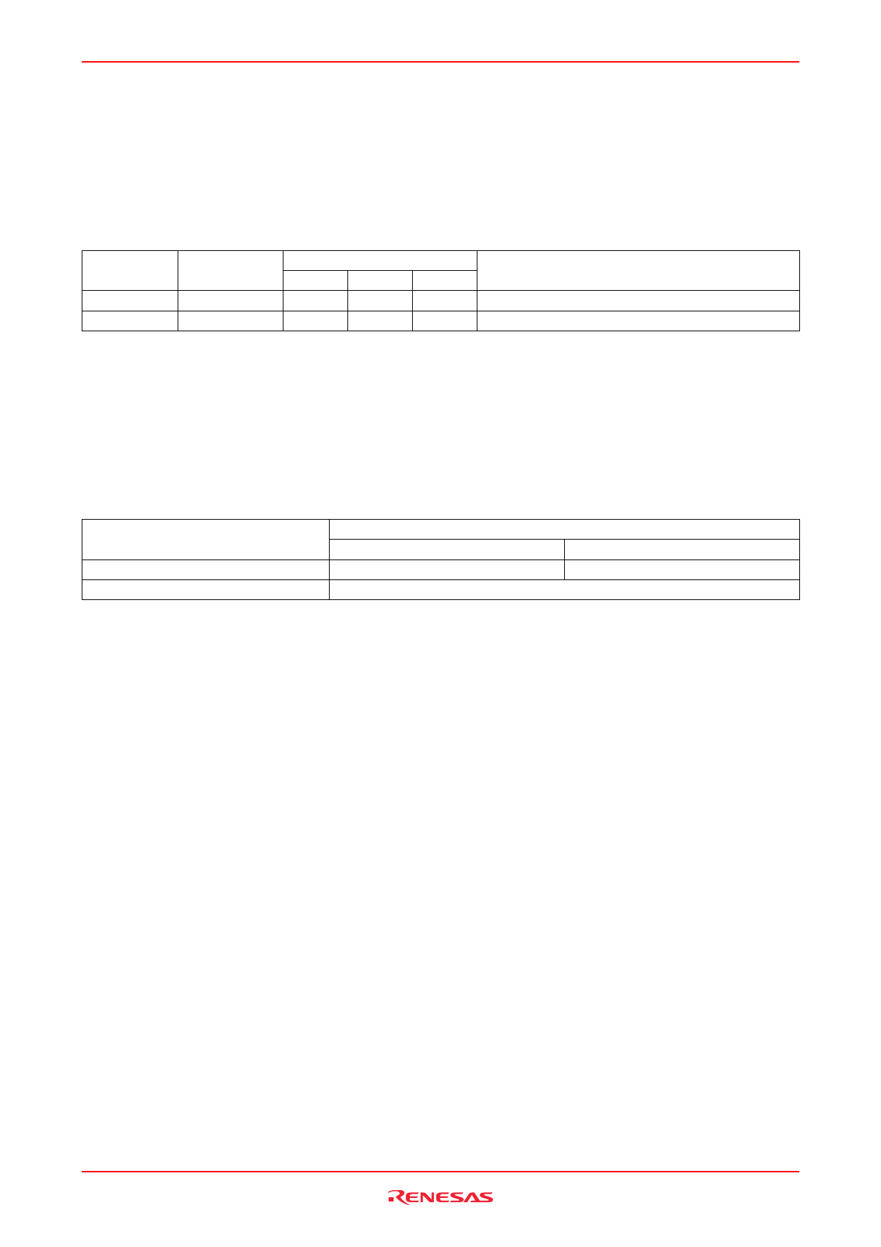
Pin Connections for A0 to A2
Max connect
Pin connection
Memory size
2k bit
4k bit
number
8
4
A2
A1
A0
Г—*1
Г—*1
Г—*1
Г—*1
Г—*1
Г—*1
Notes: 1. Г— = DonвҖҷt care (Open is also approval).
Notes
Use A0 for memory address a8
Write Protect (WP)
When the Write Protect pin (WP) is high, the write protections feature is enabled and operates as shown in the
following table. When the WP is low, write operations for all memory array are allowed. The read operation is always
activated irrespective of the WP pin status. The WP pin is internally pull-down to VSS. Write operations for all
memory array are allowed if unconnected.
Write Protect Area
WP pin status
VIH
VIL
Write protect area
2k bit
4k bit
Entire (2k bit)
Entire (4k bit)
Normal read/write operation
Rev.4.00, Jul.13.2005, page 7 of 17
Share Link: