HSP43881 查看數據表(PDF) - Intersil
零件编号
产品描述 (功能)
生产厂家
HSP43881 Datasheet PDF : 21 Pages
| |||
HSP43881
CIENB is latched internally. It enables the register for loading
after the next CLK following the onset of CIENB low. Actual
loading occurs on the second CLK following the onset of
CIENB low. Therefore, CIENB must be low during the clock
cycle immediately preceding presentation of the coefficient on
the CIN0-7 inputs. In most basic FIR operations, CIENB will be
low throughout the process, so this latching and delay
sequence is only important during the initialization phase.
When CIENB is high, the coefficients are frozen.
These registers are cleared synchronously under control of
RESET, which is latched and delayed exactly like CIENB. The
output of the C register (C0-8) is one input to 8 x 8 multiplier.
The other input to the 8 x 8 multiplier comes from the output of
the X register. This register is loaded with a data sample from
the device input signals DIN0-7 discussed above. The X
register is enabled for loading by DIENB. Loading is
synchronous with CLK when DIENB is low. Note that DIENB is
latched internally. It enables the register for loading after the
next CLK following the onset of DIENB low. Actual loading
occurs on the second CLK following the onset of DIENB low;
therefore, DIENB must be low during the clock cycle
immediately preceding presentation of the data sample on the
DIN0-7 inputs. In most basic FIR operations, DIENB will be low
throughout the process, so this latching and delay sequence is
only important during the initialization phase. When DIENB is
high, the X register is loaded with all zeros.
The multiplier is pipelined and is modeled as a multiplier core
followed by two pipeline registers, MREG0 and MREG1 (Figure
1). The multiplier output is sign extended and input as one
operand of the 26-bit adder. The other adder operand is the
output of the 26-bit accumulator. The adder output is loaded
synchronously into both the accumulator and the TREG.
The TREG loading is disabled by the cell select signal,
CELLn, where n is the cell number. The cell select is decoded
from the ADR0-2 signals to generate the TREG load enable.
The cell select is inverted and applied as the load enable to
the TREG. Operation is such that the TREG is loaded
whenever the cell is not selected. Therefore, TREG is loaded
every clock except the clock following cell selection. The
purpose of the TREG is to hold the result of a sum of products
calculation during the clock when the accumulator is cleared
to prepare for the next sum of products calculation. This
allows continuous accumulation without wasting clocks.
The accumulator is loaded with the adder output every clock
unless it is cleared. It is cleared synchronously in two ways.
When RESET and ERASE are both low, the accumulator is
cleared along with all other registers on the device. Since
ERASE and RESET are latched and delayed one clock
internally, clearing occurs on the second CLK following the
onset of both ERASE and RESET low.
The second accumulator clearing mechanism clears a single
accumulator in a selected cell. The cell select signal, CELLn,
decoded from ADR0-2 and the ERASE signal enable clearing
of the accumulator on the next CLK.
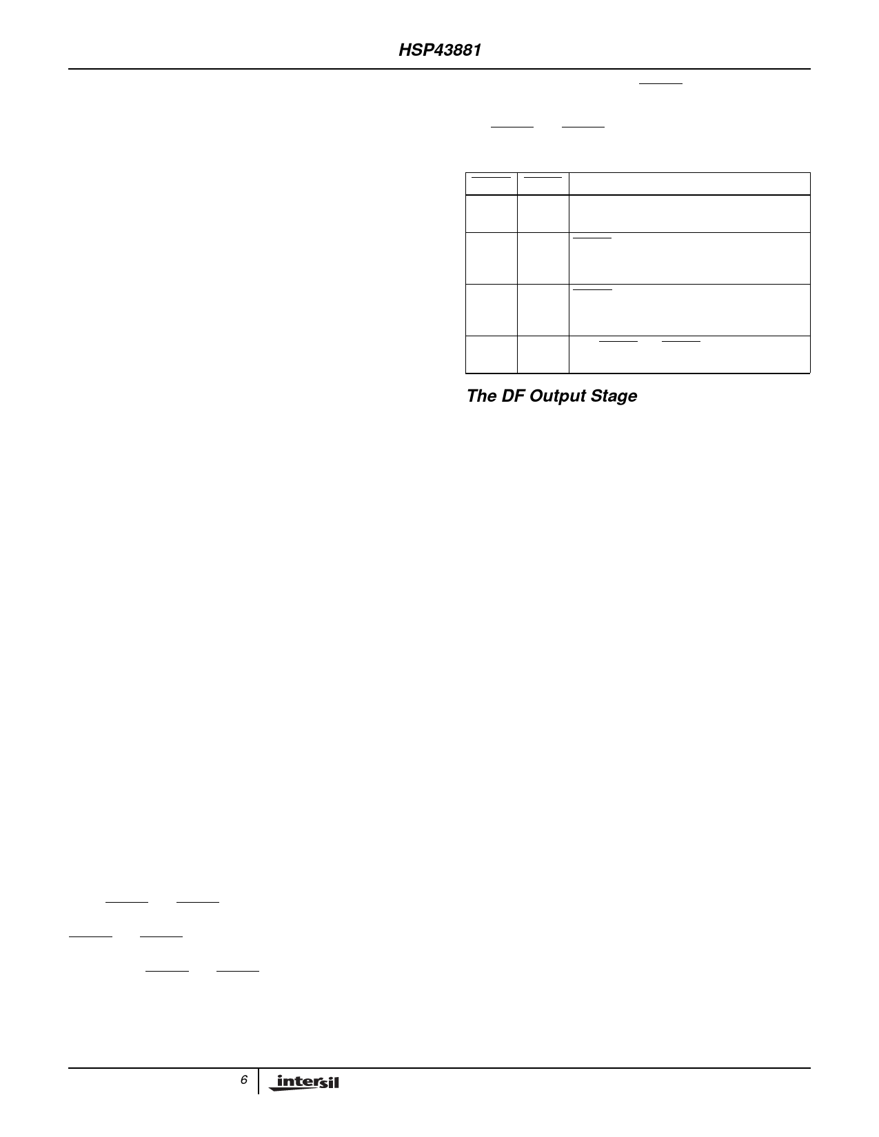
The ERASE and RESET signals clear the DF internal
registers and states as follows:
ERASE RESET
CLEARING EFFECT
1
1 No clearing occurs, internal state remains
same.
1
0 RESET only active, all registers except accu-
mulators are cleared, including the internal
pipeline registers.
0
1 ERASE only active, the accumulator whose
address is given by the ADR0-2 inputs is
cleared.
0
0 Both RESET and ERASE active, all accumula-
tors, as well as all other registers are cleared.
The DF Output Stage
The output stage consists of a 26-bit adder, 26-bit register,
feedback multiplexer from the register to the adder, an output
multiplexer and a 26-bit three-state driver stage (Figure 2).
The 26-bit output adder can add any filter cell accumulator
result to the 18 most significant bits of the output buffer. This
result is stored back in the output buffer. This operation takes
place in one clock period. The eight LSBs of the output buffer
are lost. The filter cell accumulator is selected by the ADR0-2
inputs.
The 18 MSBs of the output buffer actually pass through the
zero mux on their way to the output adder input. The zero mux
is controlled by the SHADD input signal and selects either the
output buffer 18 MSBs or all zeros for the adder input. A low
on the SHADD input selects zero. A high on the SHADD input
selects the output buffer MSBs, thus, activating the shift and
add operation. The SHADD signal is latched and delayed by
one clock internally.
6
Share Link: 