HT82V46 查看數據表(PDF) - Holtek Semiconductor
零件编号
产品描述 (功能)
生产厂家
HT82V46 Datasheet PDF : 27 Pages
| |||
HT82V46
edge of the CDS1 input signal (C1S). For input signals
that do not contain a reference level (e.g. CIS sensor
signals), non-CDS processing is used (CDS=0). In
this case, the video level is processed with respect to
the voltage on pin VRLC/VBIAS. The VRLC/VBIAS
voltage is sampled at the same time as CDS2 samples
the video level in this mode. In “WS” mode the input
video signal is always sampled on the 1st rising edge
of ADCK after CDS2 has gone low (Video Sample)
regardless of the operating mode. If in non-CDS mode
(CDS=0) the voltage on the VRLC/VBIAS pin is also
sampled at this point. In CDS-mode (CDS=1) the
position of the reference sample (C1S) can be varied,
under control of the CDSREF[1:0] register bits, as
shown in Figure11.
Line-by-Line Operation
Certain linear sensors give colour output on a line-
by-line basis. i.e. a full line of red pixels followed
by a line of green pixels followed by a line of blue
pixels. Often the sensor will have only a single output
onto which these outputs are time multiplexed. The
HT82V46 can accommodate this type of input by
setting the LNBYLN register bit high. When in this
mode the green and blue input PGAs are disabled
to save power. The analogue input signal should
be connected to the VINR pin. The offset and gain
values that are applied to the Red input channel can
be selected, by internal multiplexers, to come from
the Red, Green or Blue offset and gain registers.
This allows the gain and offset values for each of
the input colours to be setup individually at the start
of a scan. When register bit ACYC=0 the gain and
offset multiplexers are controlled via the INTM[1:0]
register bits. When INTM=00 the red offset and gain
control registers are used to control the Red input
channel, INTM=01 selects the green offset and gain
registers and INTM=10 selects the blue offset and
gain registers to control the Red input channel. When
register bit ACYC=1, ‘auto-cycling’ is enabled, and
the input channel switches to the next offset and gain
registers in the sequence when a pulse is applied to
the CDS1 input pin. The sequence is Red → Green
→ Blue → Red… offset and gain registers applied
to the single input channel. A write to the Auto-cycle
reset register (address 05h) will reset the sequence to
a known state (Red registers selected). When auto-
cycling is enabled, the CDS1 pin cannot be used to
control reset level clamping. The CLPCTL bit may be
used instead (enabled when high, disabled when low).
When auto-cycling is enabled, the CDS1 pin cannot
be used for reference sampling (i.e. CDS must be set
to 0).
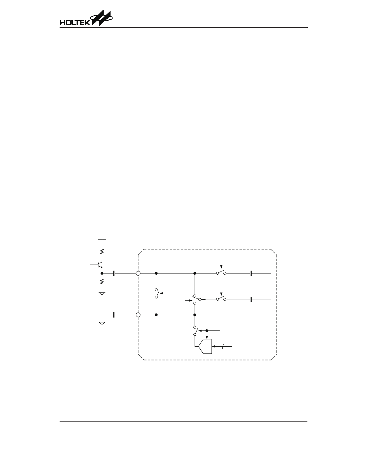
CIN
VINR
VRLC/VBIAS
CLP
CDS
C2S
Video Sample
Capacitor
C1S (CDS = 1) or
C2S (CDS = 0)
Reference Sample
=1
Capacitor
=0
RLC
DAC
CDACPD
4
CDAC[3:0]
Figure 1 CDS/non-CDS Input Configuration
Rev. 1.10
7
November 24, 2011
Share Link: 