HT9032 查看數據表(PDF) - Holtek Semiconductor
零件编号
产品描述 (功能)
生产厂家
HT9032 Datasheet PDF : 8 Pages
| |||
HT9032
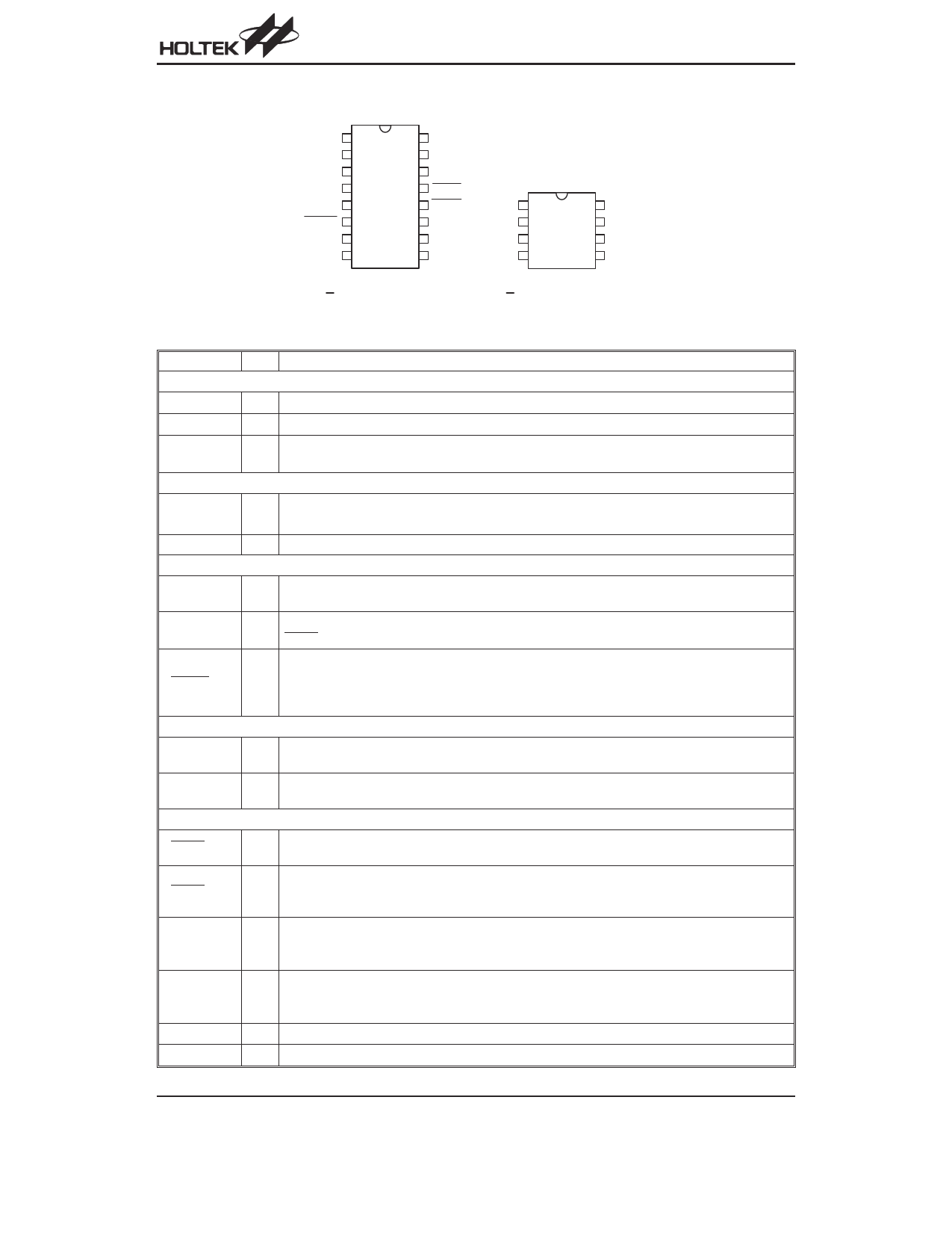
Pin Assignment
T IP 1
R IN G
2
R D ET1 3
R D ET2 4
TEST 5
R T IM E 6
PDW N
7
VSS 8
16 V D D
15 D O U TC
14 D O U T
13 C D E T
12 R D E T
11 N C
10 X 1
9 X2
H T9032C
1 6 D IP -A /S O P -A
DOUT 1
VDD 2
T IP 3
R IN G 4
8 X1
7 X2
6 VSS
5 PDW N
H T9032D
8 D IP -A /S O P -A
Pin Description
Pin Name I/O
Power Inputs
VDD
¾
VSS
¾
Description
Power-VDD is the input power for the internal logic.
Ground-VSS is ground connection for the internal logic.
PDWN
I
A logic ²1² on this pin puts the chip in power down mode. When a logic ²0² is on this pin, the
chip in power up mode. This is a Schmitt trigger input.
Clock
A crystal or ceramic resonator should be connected to this pin and X2.
X1
I
This pin may be driven from an external clock source.
X2
O A crystal or ceramic resonator should be connected to this pin and X1.
Ring Detections
RDET1
I
It detects ring energy on the line through an attenuating network and enables the oscillator and
ring detection. This is a Schmitt trigger input.
RDET2
It couples the ring signal to the precision ring detector through an attenuating network.
I RDET=²0² if a valid ring signal is detected. This is a Schmitt trigger input.
RTIME
An RC network may be connected to this pin in order to hold the pin voltage below 2.2V be-
I/O
tween the peaks of the ringing signal. This pin controls internal power up and activates the par-
tial circuitry needed to determine whether the incoming ring is valid or not. The input is a
Schmitt trigger input. The output cell structure is an NMOS output.
FSK Signal Inputs
TIP
I
RING
I
Detection Results
This input pin is connected to the tip side of the twisted pair wires. It is internally biased to 1/2
VDD when the device is in power up mode. This pin must be DC isolated from the line.
This input pin is connected to the ring side of the twisted pair wires. It is internally biased to 1/2
VDD when the device is in power up mode. This pin must be DC isolated from the line.
RDET
O
This open drain output goes low when a valid ringing signal is detected. When connected to
PDWN pin, this pin can be used for auto power up.
CDET
This open drain output goes low indicating that a valid carrier is present on the line. A hyster-
O esis is built-in to allow for a momentary drop out of the carrier. When connected to PDWN pin,
this pin can be used for auto power up.
DOUT
This pin presents the output of the demodulator when chip in power up mode. This data stream
O includes the alternate ²1² and ²0² pattern, the marking, and the data. At all other times, this pin
is held high.
DOUTC
This output presents the output of the demodulator when chip in power up mode and when an
O internal validation sequence has been successfully passed. This data stream does not include
the alternate ²1² and ²0² pattern. This pin is always held high.
TEST
O Output pin for testing purposes only.
NC
¾ No connection
Rev. 1.30
2
November 19, 2001
Share Link: 